
A timing diagram for an I2C read transaction: SCL clock, SDA with START condition, 0x30,Write bit, ACK bit, 0x03,ACK bit, 0x01, ACK bit and STOP condition
NODE ARCHIVE · REAL DIAGRAM BRIEFS
Diagram Examples from Real Visitor Prompts
Browse eligible diagrams shared by FreeDiagram visitors, inspect the exact prompts, and build your own version.
Browse 3261 real creationsCOMMUNITY OUTPUTS · EXACT PROMPTS
Timing Diagrams
Showing 1–24 of 77. No stock examples or system defaults. Choose a tool, study a real result, then reopen its prompt as your starting point.

A timing diagram for an I2C read transaction: SCL clock, SDA with START condition, 0x30,Write bit, ACK bit, 0x01,ACK bit, 0x03, ACK bit and STOP condition

A timing diagram for an I2C write transaction: SCL clock, SDA with START condition, 0x30, write bit, ACK bit, 0x03 byte,ACK bit, 0x01 byte and STOP condition

A timing diagram for an I2C write transaction: SCL clock, SDA with START condition, 0x30, write bit, ACK bit, 0x01 byte,ACK bit, 0x03 byte and STOP condition

A timing diagram for an I2C write transaction: SCL clock, SDA with START condition, 0x30, ACK bit, 0x01 byte,ACK bit, 0x03 byte and STOP condition
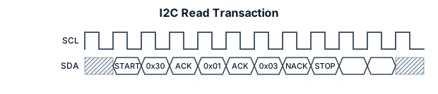
A timing diagram for an I2C read transaction: SCL clock, SDA with START condition, 0x30, ACK bit, 0x01 byte,ACK bit, 0x03 byte and STOP condition

A timing diagram for an I2C read transaction: SCL clock, SDA with START condition, 7-bit address byte, ACK bit, 0x01 byte,ACK bit, 0x03 byte and STOP condition

A timing diagram for an I2C read transaction: SCL clock, SDA with START condition, 7-bit address byte, ACK bit, data byte,ACK bit, data byte and STOP condition
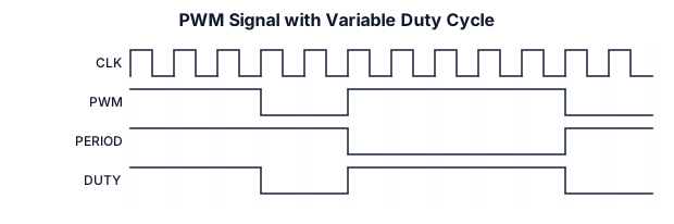
PWM signal with variable duty cycle and period annotation
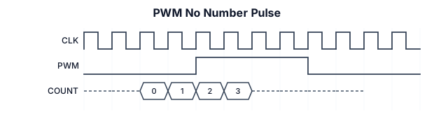
PWM diagram for no number pulse
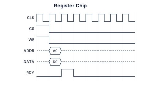
A timing diagram for Register Chip
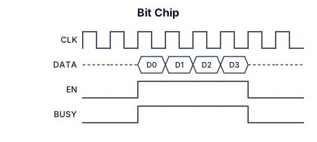
A timing diagram for Bit Chip
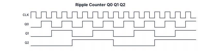
When sketching your timing diagram for 16 clock pulses, lay out four horizontal waveforms stacked vertically: CLK, Q 0 , Q 1 , and Q 2 . JPG CLK: A continuous clock pulse train with 16 distinct clock periods (square waves with uniform high and low durations). Q 0 (LSB): Changes state on every active edge (e.g., rising edge) of CLK. Has a frequency equal to CLK/2 (complete cycle every 2 clock pulses). Q 1 : Changes state whenever Q 0 has a falling edge (or when Q ˉ 0 goes active). Has a frequency equal to CLK/4 (complete cycle every 4 clock pulses). Q 2 (MSB): Changes state whenever Q 1 has a falling edge. Has a frequency equal to CLK/8 (complete cycle every 8 clock pulses, meaning it completes two full cycles across the 16 clock pulses). Note on Ripple Delay: Because this is a ripple counter, remember to show small propagation delays (slight offsets/skews) between the transition of Q 0 and the resulting toggle of Q 1 , as well as between Q 1 and Q 2 , illustrating the classic "ripple" effect characteristic of asynchronous counters.
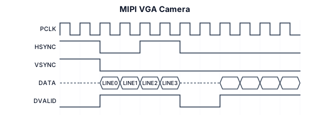
A timing diagram for MIPI VGA camera

A timing diagram for an I2C read transaction: SCL clock, SDA with START condition, 7-bit address byte, ACK bit, data byte, and STOP condition
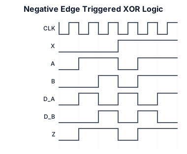
A DIAGRAM WITH D_A=X XOR B D_B = X XOR A Z = A+B. IT IS A NEGATIVE EDGE TRIGGERED CLOCK WITH X= (0,0,0,1,1,1)

A timing diagram for an I2C read transaction: SCL clock, SDA with START condition, 7-bit address byte, ACK bit, data byte, and STOP condition
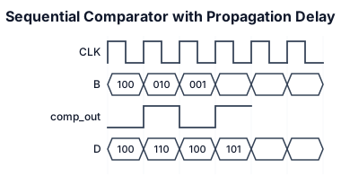
A clock signal, a 3-bit input bus B that starts at 100, a comp_out signal that starts at 0 and a D signal that starts at 100 at first; then comp is 1 which makes D(2) 1; then B is 010, D is 110, comp becomes 0, D becomes 100; B is 001, D becomes 101, comp becomes 1, D becomes 101. Every ';' is a clk rising edge. There is a propagation delay of 1/5 Tclk in each substep.

A clock signal, a 3-bit input bus B that starts at 100, a comp_out signal that starts at 0 and a D signal that starts at 100 at first; then comp is 1 which makes D(2) 1; then B is 010, D is 110, comp becomes 0, D becomes 100; B is 001, D becomes 101, comp becomes 1, D becomes 101. Every ';' is a clk rising edge. There is a propagation delay of 1/5 Tclk in each substep
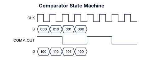
A clock signal, a 3-bit input bus B, a comp_out signal that starts at 100 and a D signal that starts at 100 at first; then comp is 1 which makes D(2) 1; then B is 010, D is 110, comp becomes 0, D becomes 100; B is 001, D becomes 101, comp becomes 1, D becomes 101. Every ';' is a clk rising edge
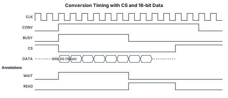
signal convs if 0 -> 1 then busy signal become 0 -> 1 it will wait for some time ~50us then it become low. once it will get 0 then CS signal goes 1->0. if CS0 -> the Data Line Have 16 bit of data. once read all CS will 0 -> 1. data will come only after CS will 1->0, if 0 ->1 no data. data is 16 bit. clk is 10Mhz
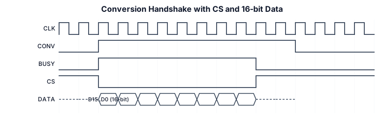
signal convs if 0 -> 1 then busy signal become 0 -> 1 it will wait for some time ~50us then it become low. once it will get 0 then CS signal goes 1->0. if CS0 -> the Data Line Have 16 bit of data. once read all CS will 0 -> 1. data will come only after CS will 1->0, if 0 ->1 no data. data is 16 bit
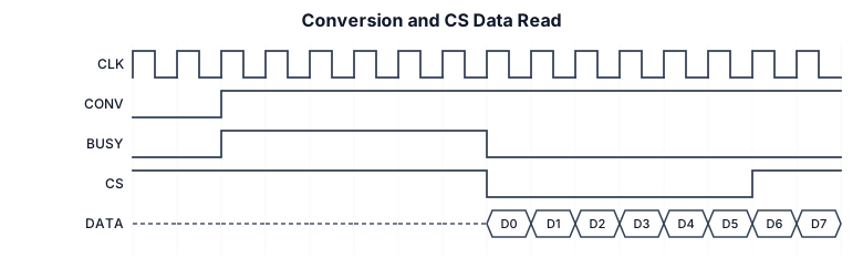
signal convs if 0 -> 1 then busy signal become 0 -> 1 it will wait for some time ~50us then it become low. once it will get 0 then CS signal goes 1->0. if CS0 -> the Data Line Have 16 bit of data. once read all CS will 0 -> 1. data will come only after CS will 1->0, if 0 ->1 no data
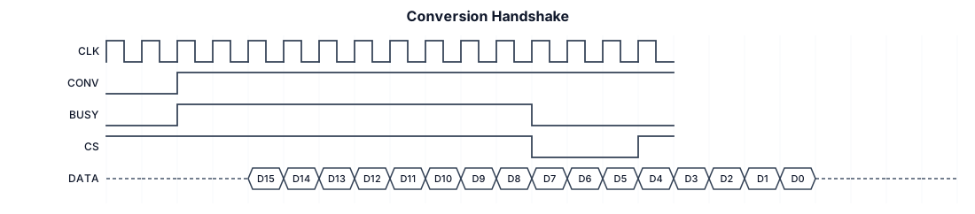
signal convs if 0 -> 1 then busy signal become 0 -> 1 it will wait for some time ~50us then it become low. once it will get 0 then CS signal goes 1->0. if CS0 -> the Data Line Have 16 bit of data. once read all CS will 0 -> 1