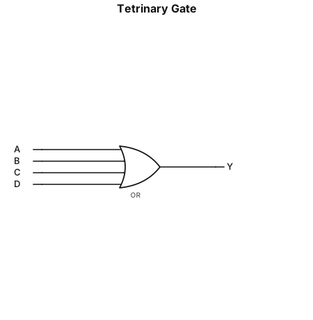
a tetrinary gate that only takes in inputs bigger than it equal to 1
NODE ARCHIVE · REAL DIAGRAM BRIEFS
Diagram Examples from Real Visitor Prompts
Browse eligible diagrams shared by FreeDiagram visitors, inspect the exact prompts, and build your own version.
Browse 3263 real creationsCOMMUNITY OUTPUTS · EXACT PROMPTS
Logic Gate
Showing 217–240 of 288. No stock examples or system defaults. Choose a tool, study a real result, then reopen its prompt as your starting point.
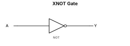
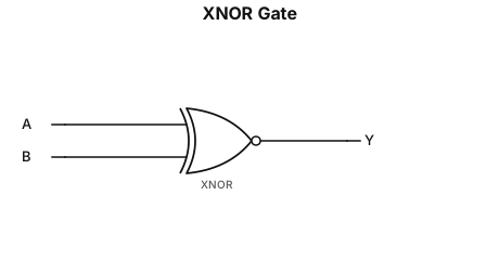
xxnor
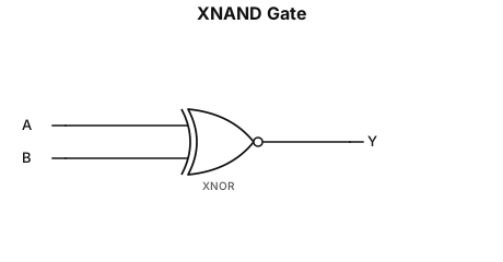
xnand
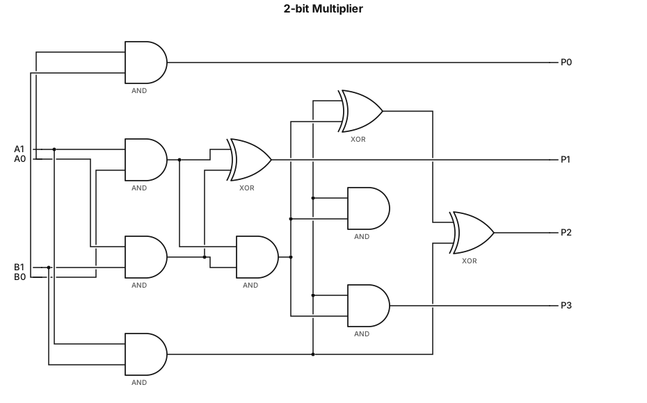
2 bit multiplier
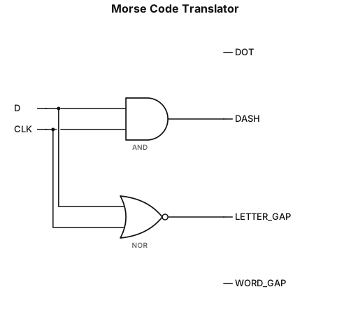
a Morse code translator
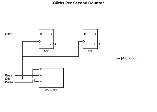
a click per sec counter
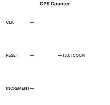
a cps counter
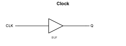
a clock
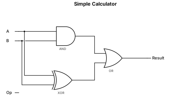
a simple calculator
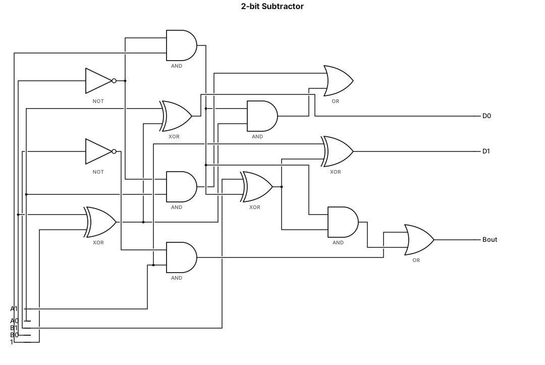
2 bit subtractor
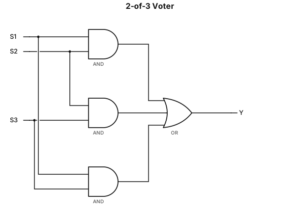
a thing that turns on only if 2/3 switches are on
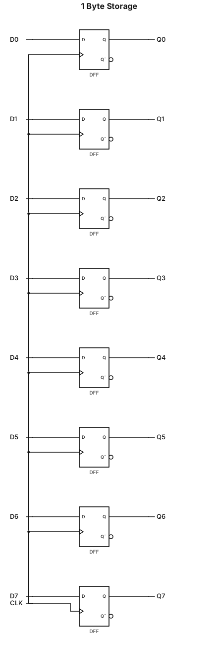
a 1 byte storage
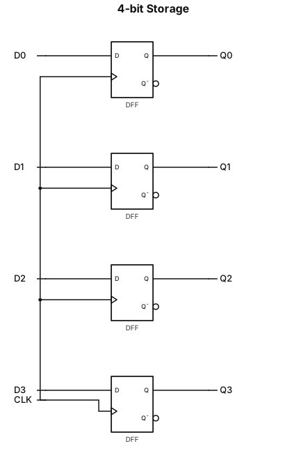
a 4 bit storage
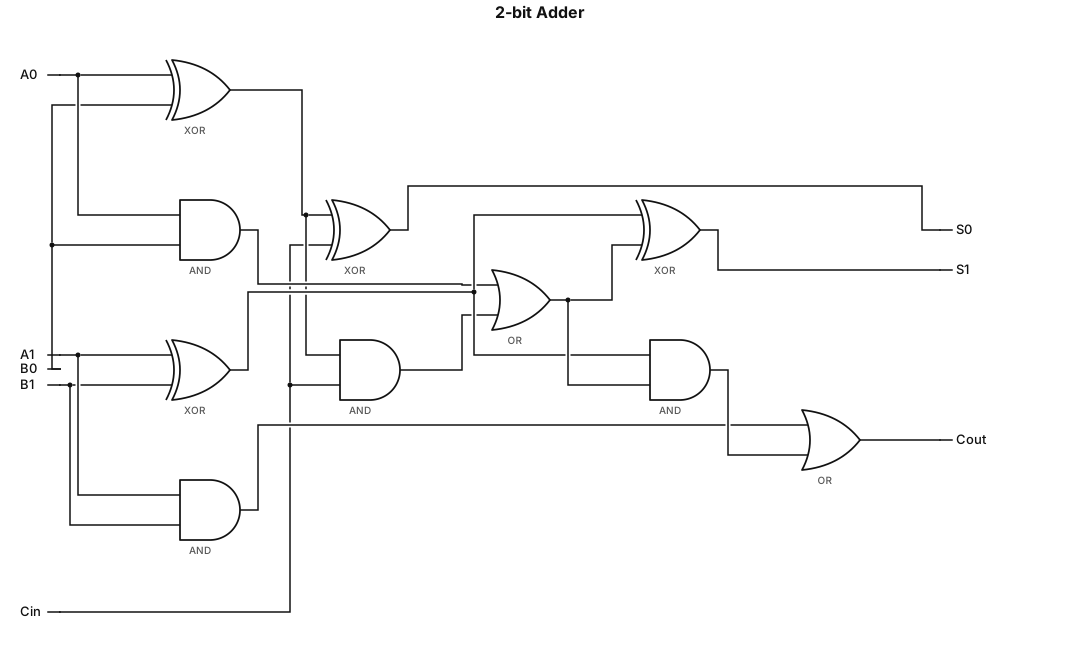
a 2 bit adder
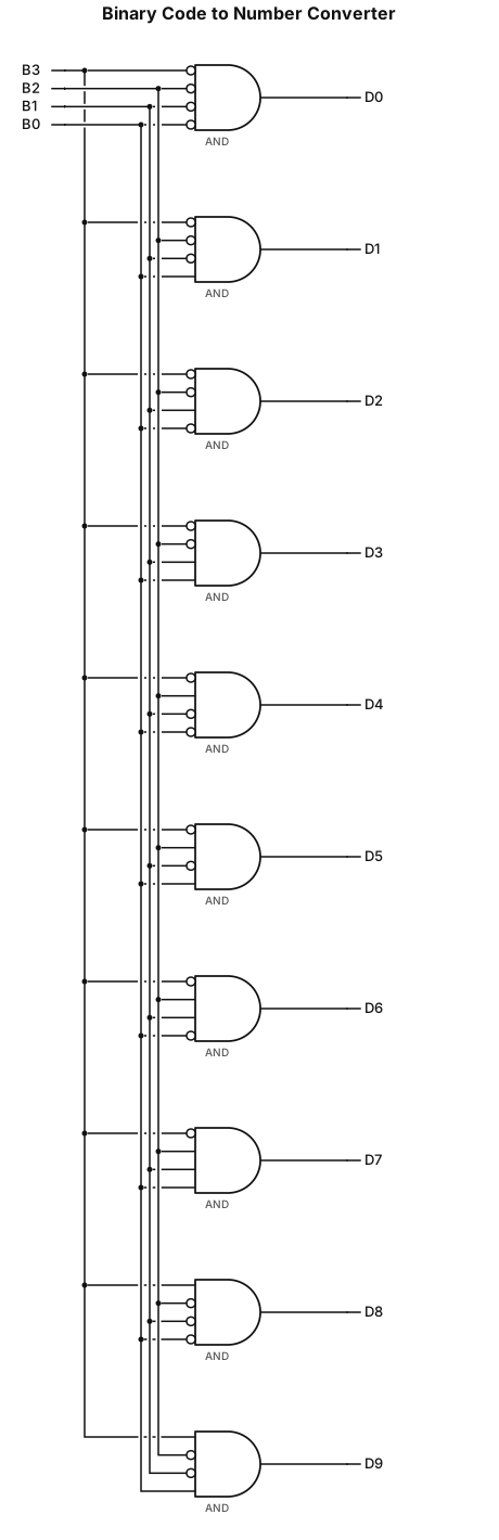
a binary code to number
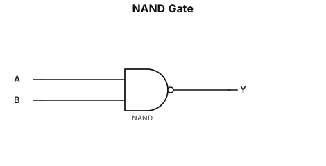
nand gate with two input and one output
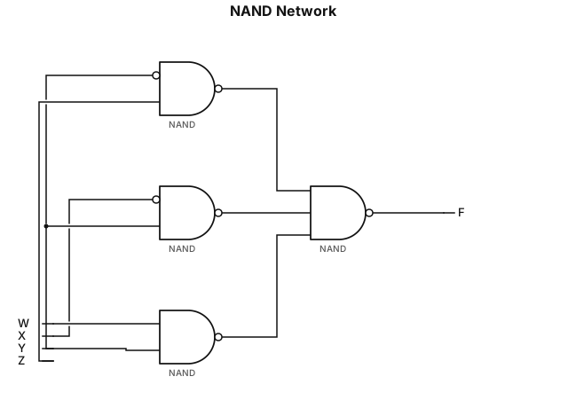
(Y' NAND Z) NAND (X' NAND Y) NAND (W NAND Y)
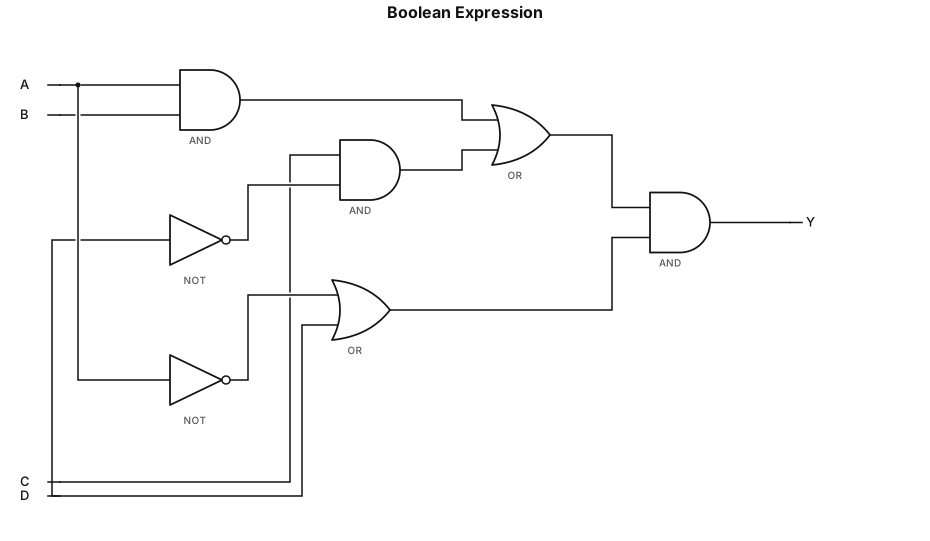
((A * B) + (C * NOT D)) * (NOT A + D)
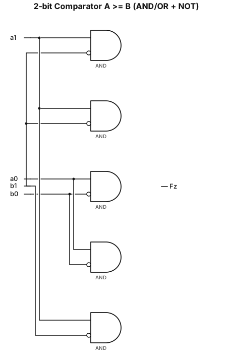
Let A = a1a0 and B = b1b0 be 2-bit unsigned binary numbers. Design a circuit with inputs a1, a0, b1, b0 and output Fz such that: Fz = 1 if and only if A ≥ B. Draw TWO circuit diagrams: (a) Realize the circuit using only AND2 and OR2 gates, with NOT gates allowed for complemented inputs. (b) Realize the circuit using only NAND2 and NOR2 gates. Clearly label every input, intermediate signal, gate, and final output Fz.
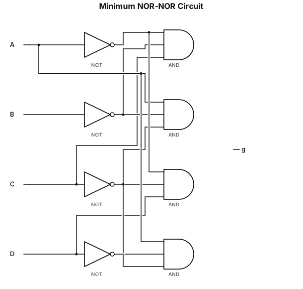
g=A′B′C+AB′C′+A′C′D+AC′D′ draw: Minimum NOR-NOR circuit
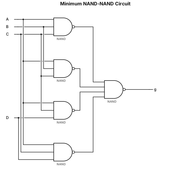
g=A′B′C+AB′C′+A′C′D+AC′D′ draw: Minimum NAND-NAND circuit
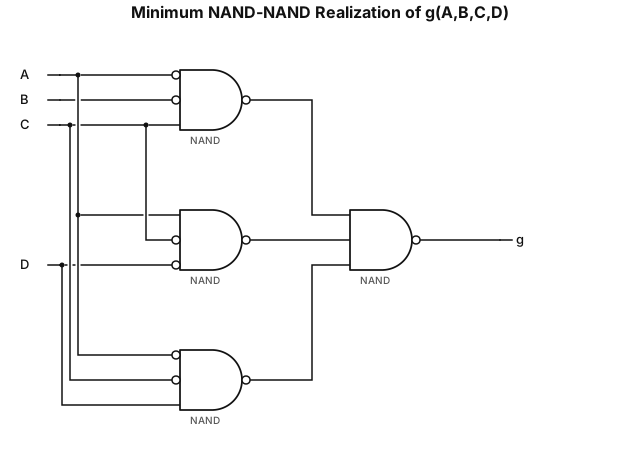
Design the minimum two-level NAND-NAND and NOR-NOR realizations of: g(A,B,C,D) = Σm(2,3,6,8,9,12) Simplify the Boolean function first using a Karnaugh map. Then draw: Minimum NAND-NAND circuit or Problem 3: $$ g(A,B,C,D)=\Sigma m(2,3,6,8,9,12) $$ Minimum SOP equation for NAND-NAND: g= A B C+A B C + A C D+A C D Use only two logic levels and clearly label all complemented inputs, intermediate outputs, and final output g.
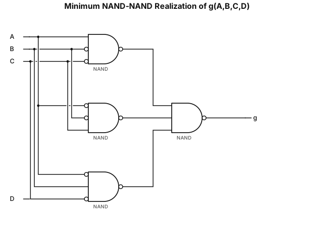
Design the minimum two-level NAND-NAND and NOR-NOR realizations of: g(A,B,C,D) = Σm(2,3,6,8,9,12) Simplify the Boolean function first using a Karnaugh map. Then draw: Minimum NAND-NAND circuit Use only two logic levels and clearly label all complemented inputs, intermediate outputs, and final output g.