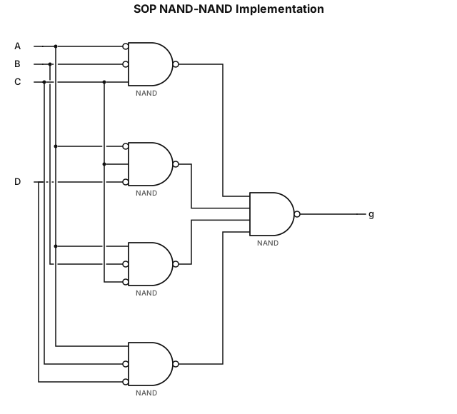
Function: g ( A , B , C , D ) = Σ m ( 2 , 3 , 6 , 8 , 9 , 12 ) g(A,B,C,D)=Σm(2,3,6,8,9,12) Minimum SOP Form (for NAND-NAND): g = A ′ B ′ C + A ′ C D ′ + A B ′ C ′ + A C ′ D ′ g=A ′ B ′ C+A ′ CD ′ +AB ′ C ′ +AC ′ D ′ do not put NOT Gates, simplify wiring
NODE ARCHIVE · REAL DIAGRAM BRIEFS
Diagram Examples from Real Visitor Prompts
Browse eligible diagrams shared by FreeDiagram visitors, inspect the exact prompts, and build your own version.
Browse 3264 real creationsCOMMUNITY OUTPUTS · EXACT PROMPTS
Logic Gate
Showing 241–264 of 288. No stock examples or system defaults. Choose a tool, study a real result, then reopen its prompt as your starting point.
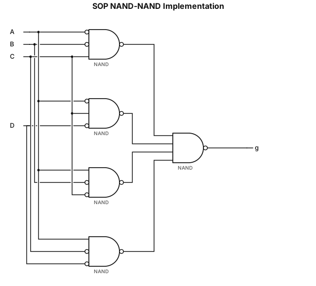
Function: g ( A , B , C , D ) = Σ m ( 2 , 3 , 6 , 8 , 9 , 12 ) g(A,B,C,D)=Σm(2,3,6,8,9,12) Minimum SOP Form (for NAND-NAND): g = A ′ B ′ C + A ′ C D ′ + A B ′ C ′ + A C ′ D ′ g=A ′ B ′ C+A ′ CD ′ +AB ′ C ′ +AC ′ D ′ do not put NOT Gates
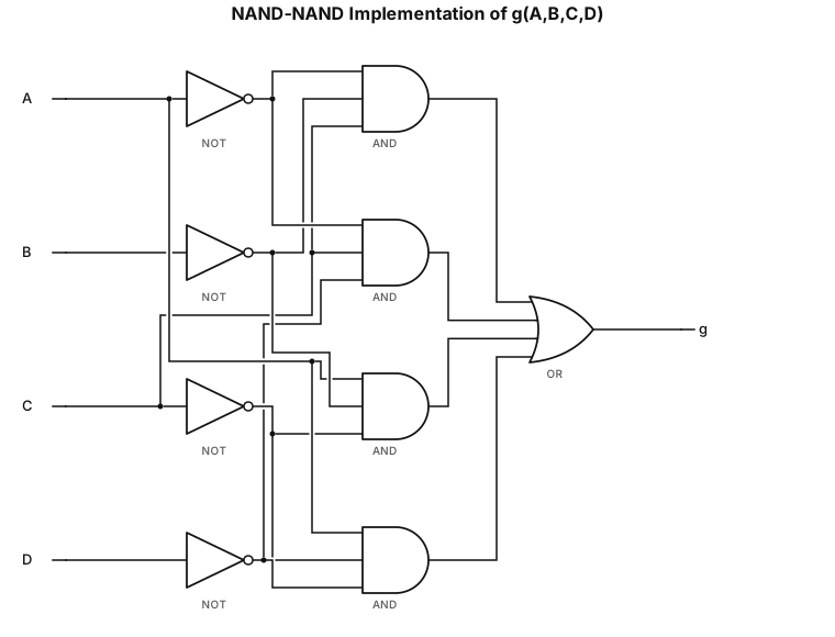
Function: g ( A , B , C , D ) = Σ m ( 2 , 3 , 6 , 8 , 9 , 12 ) g(A,B,C,D)=Σm(2,3,6,8,9,12) Minimum SOP Form (for NAND-NAND): g = A ′ B ′ C + A ′ C D ′ + A B ′ C ′ + A C ′ D ′ g=A ′ B ′ C+A ′ CD ′ +AB ′ C ′ +AC ′ D ′
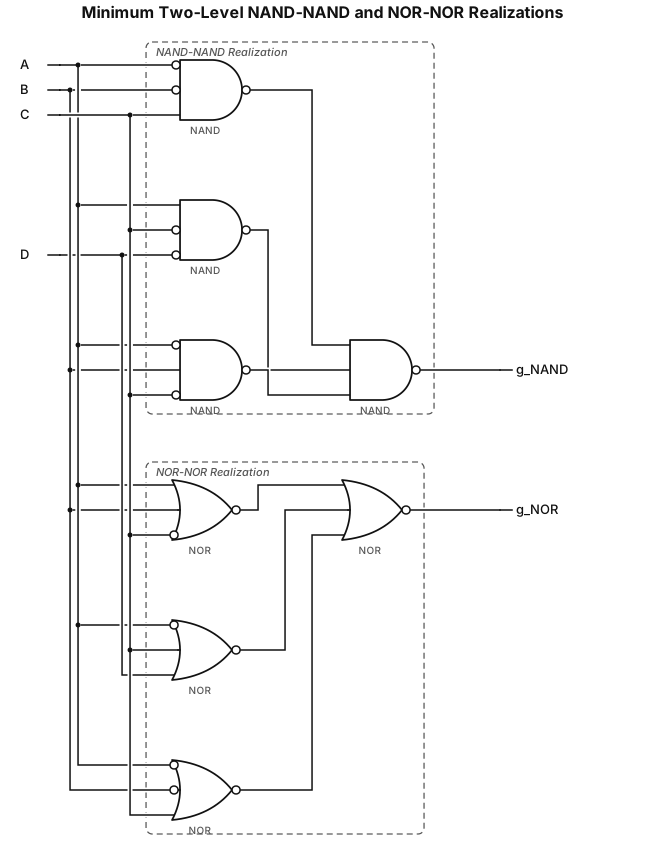
Design the minimum two-level NAND-NAND and NOR-NOR realizations of: g(A,B,C,D) = Σm(2,3,6,8,9,12) Simplify the Boolean function first using a Karnaugh map. Then draw: 1. Minimum NAND-NAND circuit 2. Minimum NOR-NOR circuit Use only two logic levels and clearly label all complemented inputs, intermediate outputs, and final output g.
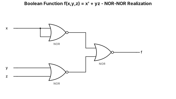
Design the Boolean function f(x,y,z) = x' + yz. Draw TWO circuit diagrams: 1. NOR-NOR realization Use standard logic-gate symbols and clearly label all wires and the final output f.
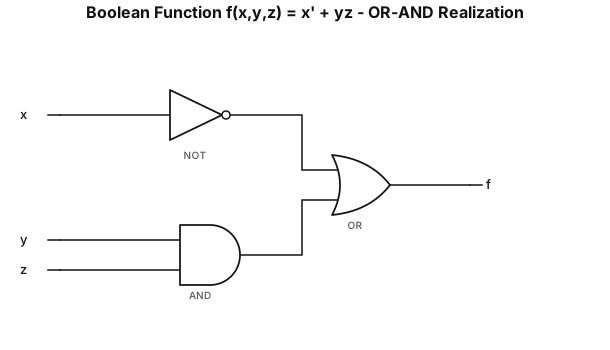
Design the Boolean function f(x,y,z) = x' + yz. Draw TWO circuit diagrams: 1. OR-AND realization Use standard logic-gate symbols and clearly label all wires and the final output f.
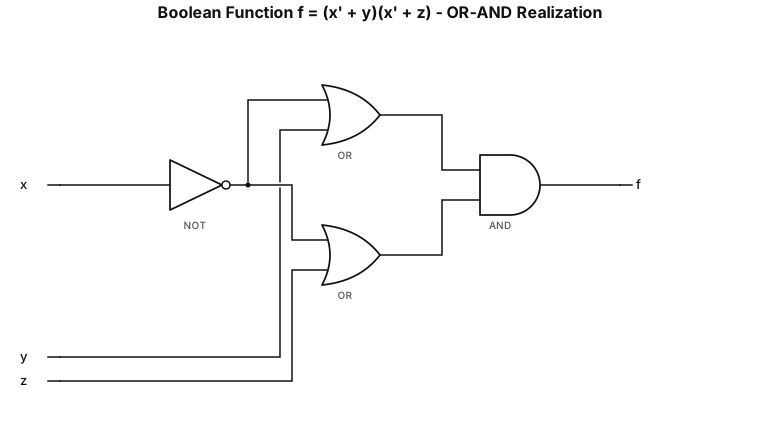
Design the Boolean function f(x,y,z) = x' + yz. First rewrite it as: f = (x' + y)(x' + z) Draw TWO circuit diagrams: 1. OR-AND realization Use standard logic-gate symbols and clearly label all wires and the final output f.
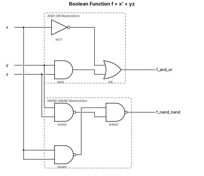
Design the Boolean function f(x,y,z) = x' + yz. Draw TWO circuit diagrams: 1. AND-OR realization 2. NAND-NAND realization Use standard logic-gate symbols, clearly label all inputs, intermediate outputs, and final output f.
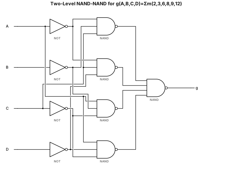
Draw a standard two-level NAND-NAND circuit for g(A,B,C,D)=Σm(2,3,6,8,9,12). First use four separate NOT gates to create A’, B’, C’, and D’. Then use exactly four 3-input NAND gates: NAND1 inputs A’, B’, C; NAND2 inputs A’, C, D’; NAND3 inputs A, B’, C’; NAND4 inputs A, C’, D’. Connect the outputs of these four NAND gates to one final 4-input NAND gate producing g. Do NOT use input bubbles. Use explicit NOT gate symbols for all complemented variables. Label every signal clearly and clean up the crossing wires
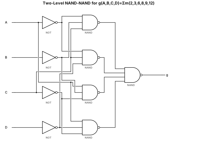
Draw a standard two-level NAND-NAND circuit for g(A,B,C,D)=Σm(2,3,6,8,9,12). First use four separate NOT gates to create A’, B’, C’, and D’. Then use exactly four 3-input NAND gates: NAND1 inputs A’, B’, C; NAND2 inputs A’, C, D’; NAND3 inputs A, B’, C’; NAND4 inputs A, C’, D’. Connect the outputs of these four NAND gates to one final 4-input NAND gate producing g. Do NOT use input bubbles. Use explicit NOT gate symbols for all complemented variables. Label every signal clearly.
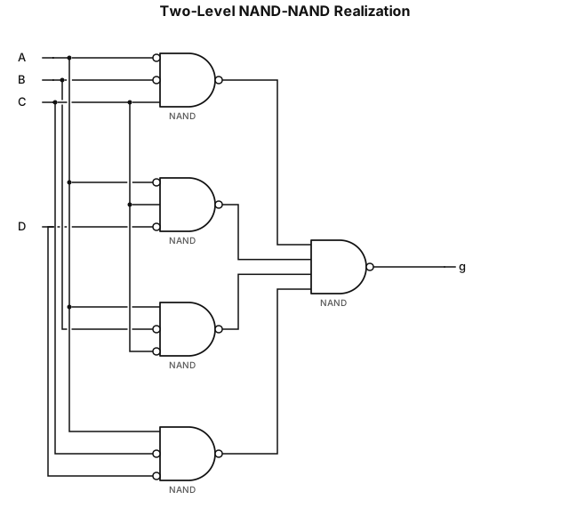
Draw a minimum two-level NAND-NAND realization for g(A,B,C,D)=\Sigma m(2,3,6,8,9,12). Use the SOP expression g=A'B'C+A'CD'+AB'C'+AC'D'. Draw exactly four first-level NAND gates, one for each product term, followed by one final NAND gate. Clearly label A, B, C, D and all complemented inputs.
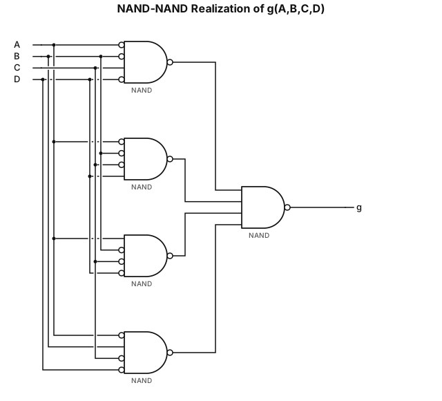
3. Design minimum two-level NAND-NAND and NOR-NOR realizations of the function g(A, B, C, D) = ∑m(2,3,6,8,9,12)
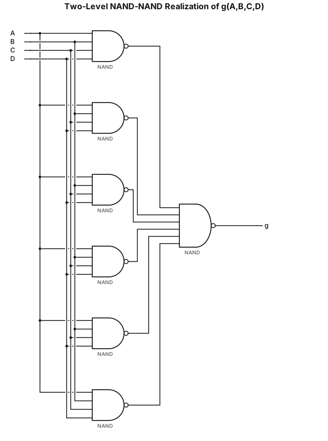
Design minimum two-level NAND-NAND realizations of the function g(A, B, C, D) = ∑m(2,3,6,8,9,12)
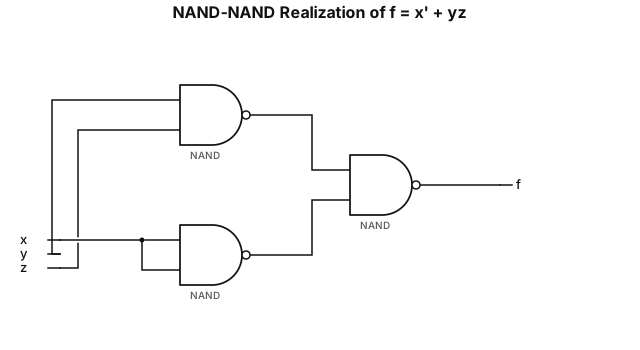
NAND-NAND realizations of f=x’+yz
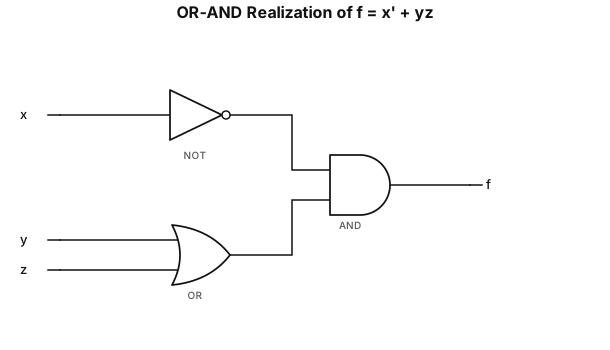
OR-AND realizations of f=x’+yz
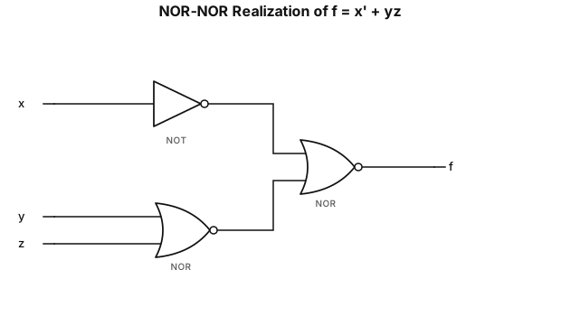
NOR-NOR realizations of f=x’+yz
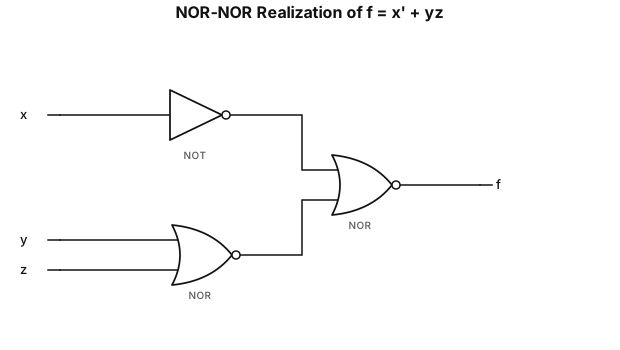
Draw NOR-NOR realizations of f=xbar+yz
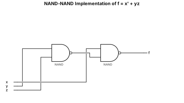
NAND-NAND of f=xbar+yz
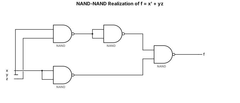
NAND-NAND realizations of the logic function f(x, y, z) = xbar+ yz. Draw the circuit diagrams.
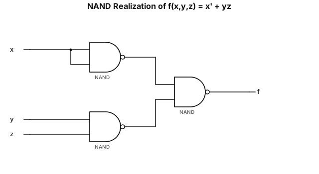
NAND nandrealizations of the logic function f(x, y, z) = xbar+ yz. Draw the circuit diagrams.
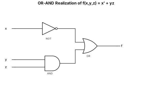
OR-AND realizations of the logic function f(x, y, z) = xbar+ yz. Draw the circuit diagrams.
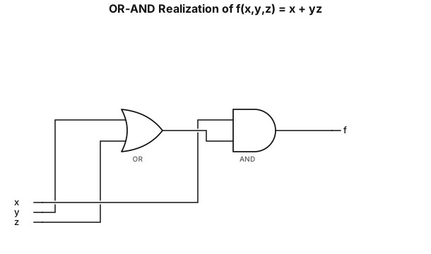
OR-AND realizations of the logic function f(x, y, z) = x + yz. Draw the circuit diagrams.
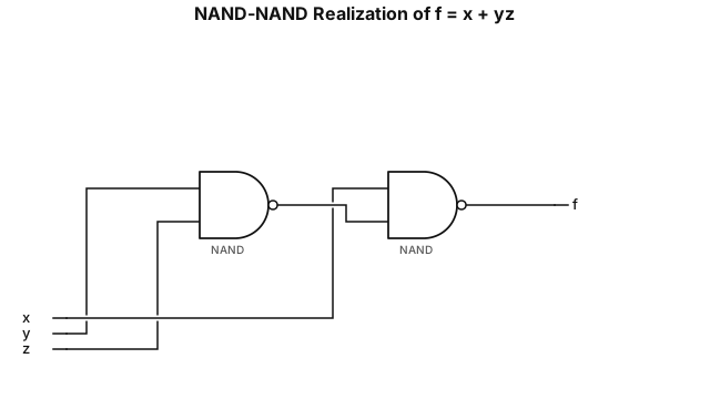
NAND-NAND realizations of the logic function f(x, y, z) = x + yz. Draw the circuit diagrams.
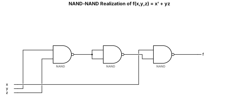
Design NAND-NAND realizations of the logic function f(x, y, z) = xbar+ yz. Draw the circuit diagrams. Make it clear please