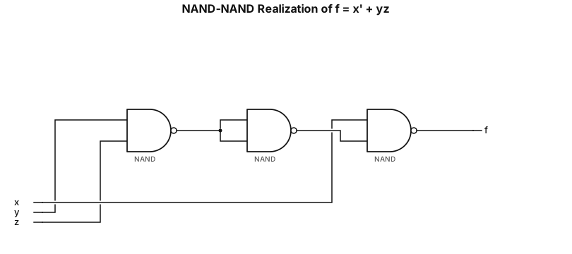
Design NAND-NAND realizations of the logic function f(x, y, z) = xbar+ yz. Draw the circuit diagrams.
NODE ARCHIVE · REAL DIAGRAM BRIEFS
Diagram Examples from Real Visitor Prompts
Browse eligible diagrams shared by FreeDiagram visitors, inspect the exact prompts, and build your own version.
Browse 3265 real creationsCOMMUNITY OUTPUTS · EXACT PROMPTS
Logic Gate
Showing 265–288 of 288. No stock examples or system defaults. Choose a tool, study a real result, then reopen its prompt as your starting point.
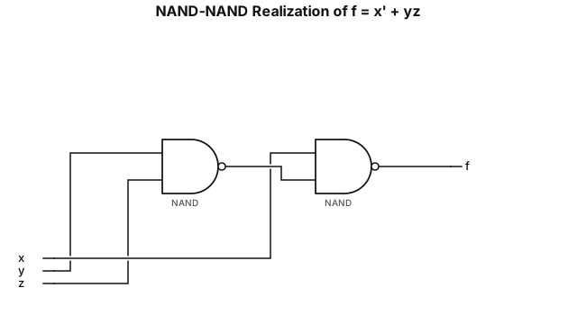
Design NAND-NAND realizations of the logic function f(x, y, z) = xbar + yz. Draw the circuit diagrams.
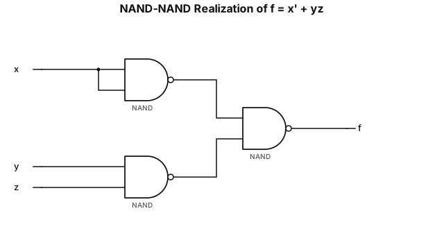
Design NAND- NAND realizations of the logic function f(x, y, z) = xbar + yz. Draw the circuit diagrams.
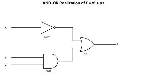
Design AND-OR realizations of the logic function f(x, y, z) = xbar + yz. Draw the circuit diagrams.
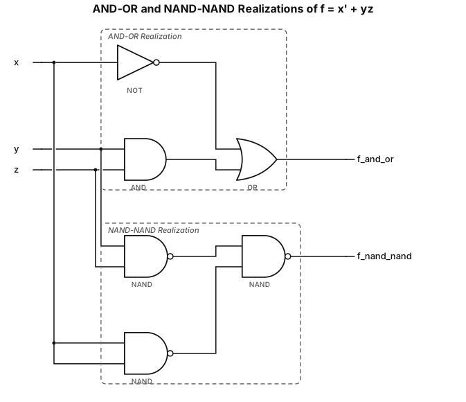
Design AND-OR and NAND-NAND realizations of the logic function f(x, y, z) = xbar + yz. Draw the circuit diagrams.
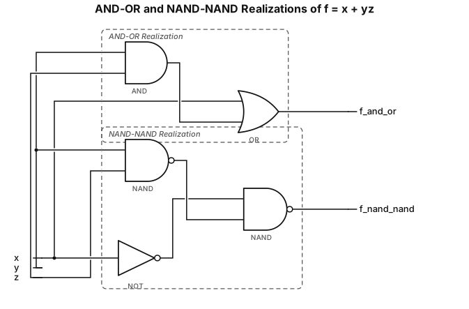
Design AND-OR and NAND-NAND realizations of the logic function f(x, y, z) = x + yz. Draw the circuit diagrams.
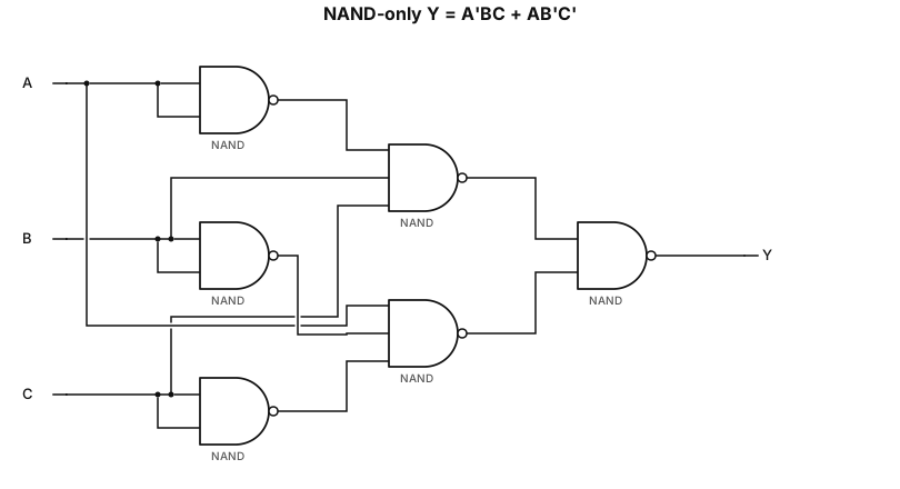
NAND-only implementation of Y = A'BC + AB'C'
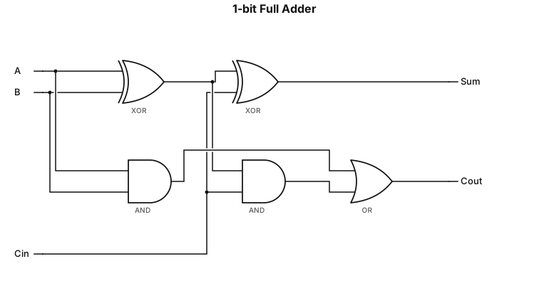
A logic gate circuit for a 1-bit full adder using AND, OR, and XOR gates with inputs A, B, and carry-in, and outputs sum and carry-out.
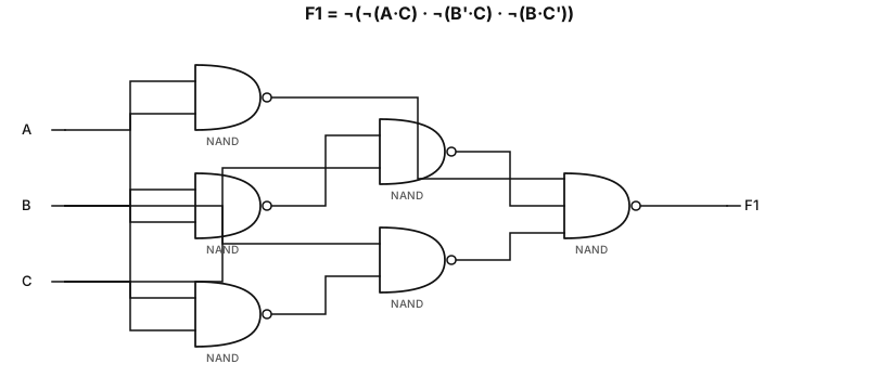
enera un diagrama de circuito lógico digital correspondiente exactamente a la siguiente función booleana: F₁ = ¬(¬(A·C) · ¬(B'·C) · ¬(B·C')) Construye el circuito utilizando únicamente compuertas NAND, respetando exactamente las negaciones de la expresión. Coloca las entradas A, B y C en el lado izquierdo. Para A·C, utiliza una compuerta NAND. Para B'·C, primero genera B' mediante una NAND usada como inversor y luego conecta B' y C a otra NAND. Para B·C', primero genera C' mediante una NAND usada como inversor y luego conecta B y C' a otra NAND. Conecta las tres salidas anteriores a una NAND final de 3 entradas, que produzca F₁. Coloca la salida F₁ en el extremo derecho. Todas las conexiones deben ser claras, ordenadas y horizontales. Usa símbolos estándar de compuertas lógicas digitales. No agregues compuertas que no sean necesarias. Coloca las etiquetas A, B, C, B', C' y F₁ claramente. El resultado debe parecer un diagrama de circuito de compuertas lógicas para una tarea universitaria, no una infografía. Fondo blanco, líneas negras/grises, símbolos limpios y texto perfectamente legible.
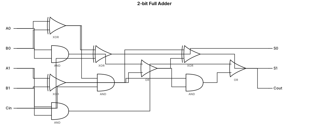
A logic gate circuit for a 2-bit full adder using AND, OR, and XOR gates with inputs A, B, and carry-in, and outputs sum and carry-out
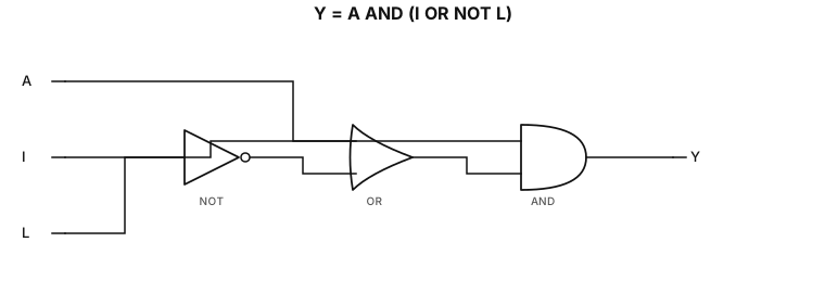
Create a logic gate diagram for Y = A AND (I OR NOT L). L must connect only to the NOT gate. The NOT gate output L′ and input I must connect to the two inputs of the OR gate. The OR gate output and input A must connect to the two inputs of the AND gate. The AND gate output is Y. Do not connect I and L together, and do not connect A to the OR gate.
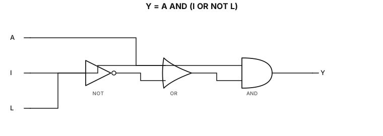
Create a logic gate diagram for Y = A AND (I OR NOT L). Use one NOT gate on L, feed L′ and I into an OR gate, then feed the OR output and A into an AND gate, with output Y.
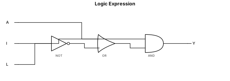
A AND (I OR NOT L)
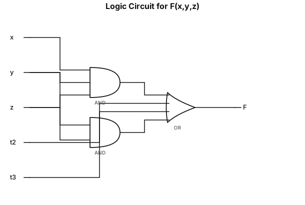
Draw the logic circuit for the following expression, assuming two-input gates: F(x, y, z) = xyz + xy' + x'y'z + yz Draw and label the circuit clearly. Show the gate structure needed to implement each product term and the final OR operation.
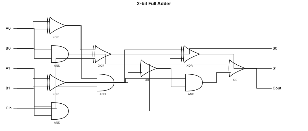
A logic gate circuit for a 2-bit full adder using AND, OR, and XOR gates with inputs A, B, and carry-in, and outputs sum and carry-out
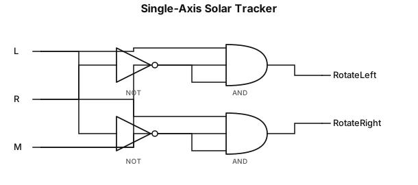
Create a simple single-axis solar tracking logic-gate diagram. Use two light sensors: Left Sensor (L) and Right Sensor (R), plus Motor Enable (M). The motor rotates left when L=1, M=1, and R=0. The motor rotates right when R=1, M=1, and L=0. Use NOT gates to invert the opposite sensor and AND gates to produce Rotate Left and Rotate Right outputs. Use standard logic-gate symbols, black lines, white background, and labels similar to a school engineering schematic.
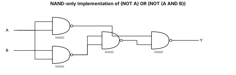
NAND-only implementation of the expression (NOT A) OR (NOT (A AND B))
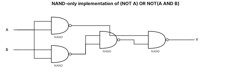
NAND-only implementation of the expression (NOT A) OR NOT(A AND B)
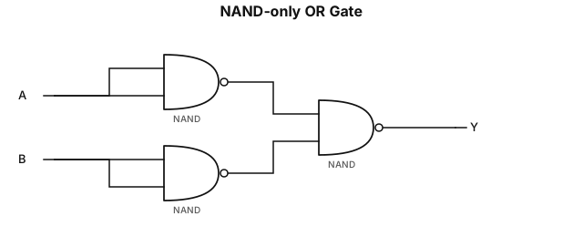
NAND-only implementation of OR gate
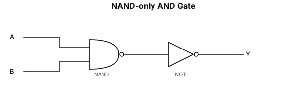
NAND-only implementation of AND gate
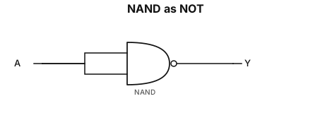
NAND-only implementation of NOT gate
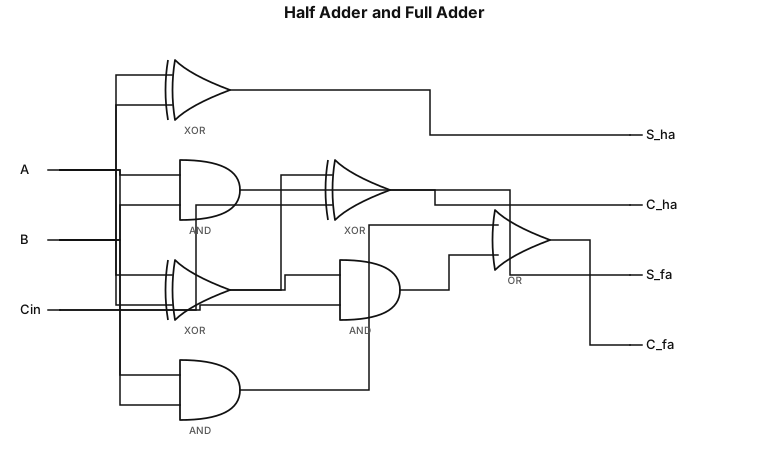
design a half adder and full adder using logic gates
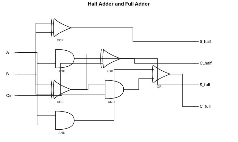
design a half adder abd full adder using logic gates
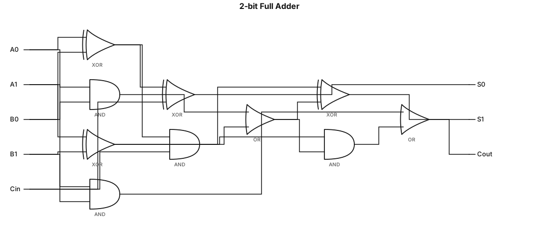
A logic gate circuit for a 2-bit full adder using AND, OR, and XOR gates with inputs A, B, and carry-in, and outputs sum and carry-out