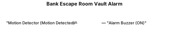
Create a simple, clearly labelled logic diagram titled "Bank Escape Room Vault Alarm". Show one input labelled "Motion Detector (Motion Detected)" connected by a line to an OR gate is not needed. Instead, use a direct connection from the motion detector to an output labelled "Alarm Buzzer (ON)". Use standard electronic diagram symbols, clear connecting lines, a white background, and a clean school-assignment style. Make sure the connection between the motion detector and the alarm buzzer is clearly visible.
NODE ARCHIVE · REAL DIAGRAM BRIEFS
Diagram Examples from Real Visitor Prompts
Browse eligible diagrams shared by FreeDiagram visitors, inspect the exact prompts, and build your own version.
Browse 3261 real creationsCOMMUNITY OUTPUTS · EXACT PROMPTS
Logic Gate
Showing 25–48 of 288. No stock examples or system defaults. Choose a tool, study a real result, then reopen its prompt as your starting point.
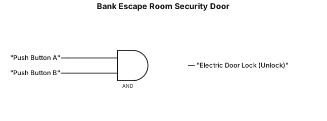
Create a simple, clearly labelled logic gate diagram for a bank escape room security door. Show two inputs labelled Push Button A and Push Button B. Connect both inputs to a single AND gate. Connect the AND gate output to an output labelled Electric Door Lock (Unlock). Use standard logic gate symbols, clear connecting lines, and a white background.
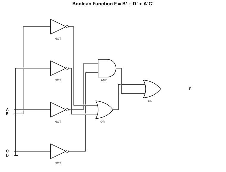
A logic gate circuit using AND, OR, and NOT gates with inputs A, B, C and D for this function: F = (B')+(D')+(A'C')
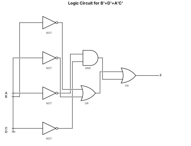
A logic gate circuit using AND, OR, and NOT gates with inputs A, B, C and D for this function: B'+D'+A'C'
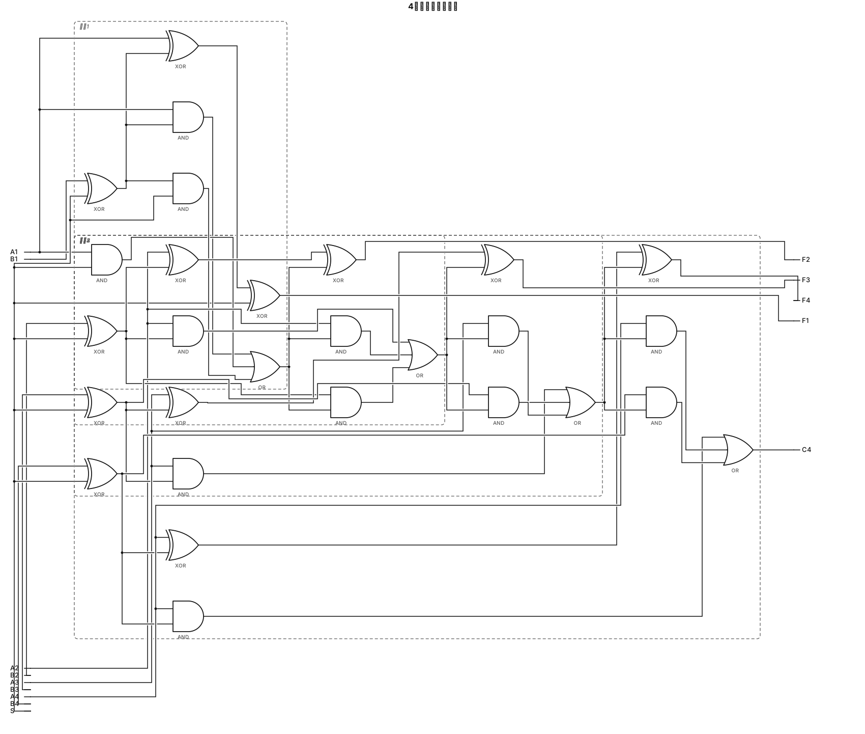
黑白线稿数字逻辑电路图,仅使用XOR异或门、AND与门、OR或门,不能使用全加器方块。 4个完全相同的可级联1位加减单元,从低位到高位依次为单元1、单元2、单元3、单元4。 每个单元输入:Ai, Bi, S, Cin;输出Fi, Cout。 每个单元内部:Bi和S送入XOR门,输出Pi;全加电路由2个XOR、3个AND、1个OR组成。 3个AND门的输入必须全部接好: AND1:Ai 和 Pi AND2:Ai 和 Cin AND3:Pi 和 Cin 三个AND的输出全部接到后面同一个OR门,没有悬空引脚,没有多余孤立门。 所有单元共用同一个控制信号S。 单元1(最低位,A1,B1):Cin = S,输出F1,Cout引出连线C1; 单元2(A2,B2):Cin接单元1引出的C1,输出F2,Cout引出连线C2; 单元3(A3,B3):Cin接单元2引出的C2,输出F3,Cout引出连线C3; 单元4(最高位,A4,B4):Cin接单元3引出的C3,输出F4,Cout作为整个电路唯一对外输出C4; 标注全部信号:A4,A3,A2,A1,B4,B3,B2,B1,S,F4,F3,F2,F1,C4。内部进位C1、C2、C3只在单元之间的连线上标注,不作为对外输出。 重点:所有逻辑门的输入输出引脚全部连线,不允许出现孤立、悬空的AND、XOR门。线条规整,无多余装饰,计算机组成原理作业图。
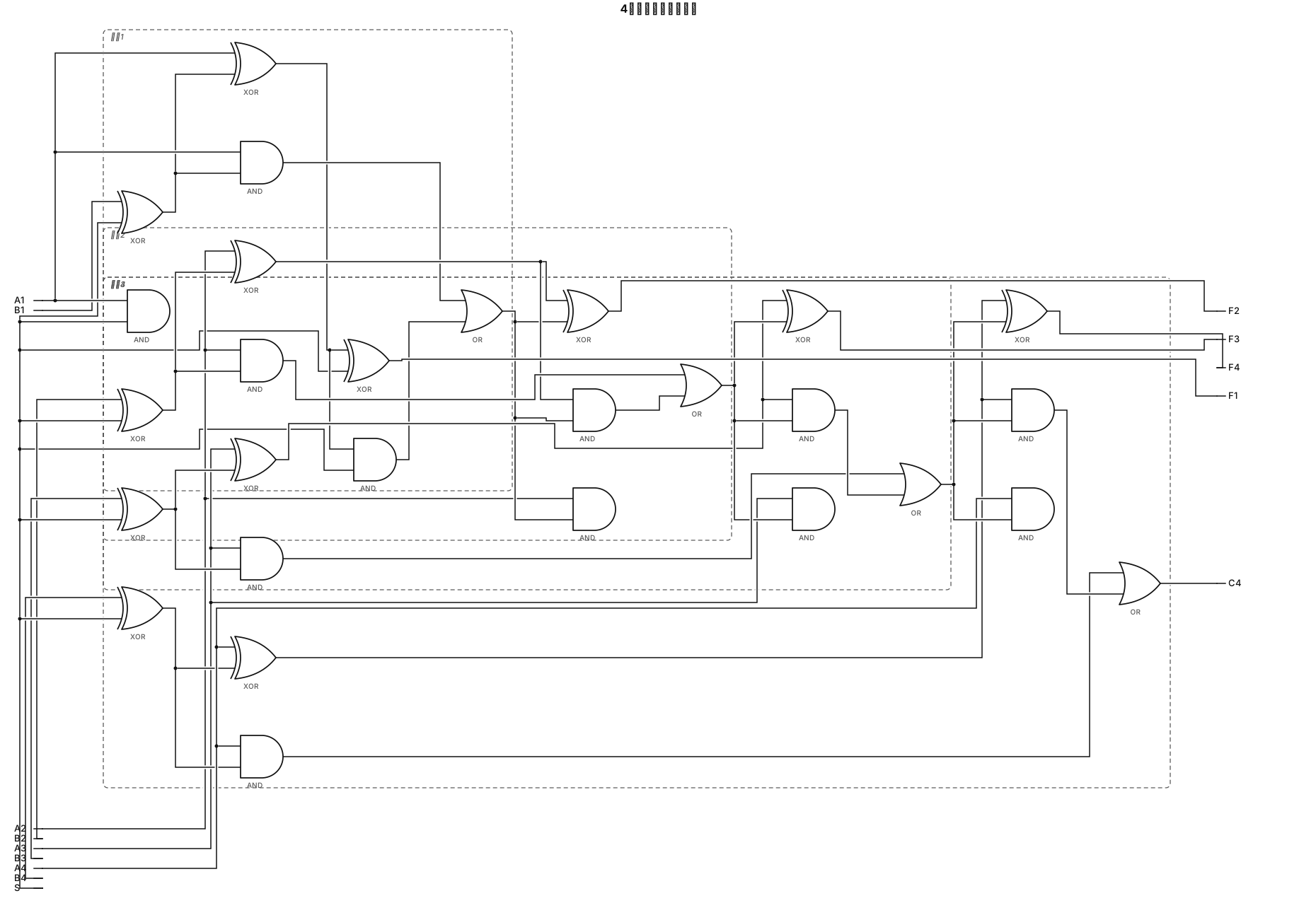
黑白线稿数字逻辑电路图,仅使用XOR异或门、AND与门、OR或门,不能使用全加器方块。 4个完全相同的可级联1位加减单元,从低位到高位依次为单元1、单元2、单元3、单元4。 每个单元输入:Ai, Bi, S, Cin;输出Fi, Cout。 每个单元内部:Bi和S送入XOR门,输出送入全加电路;全加电路由2个XOR、3个AND、1个OR组成。 所有单元共用同一个控制信号S。 单元1(最低位,A1,B1):Cin = S,输出F1,Cout引出连线C1; 单元2(A2,B2):Cin接单元1引出的C1,输出F2,Cout引出连线C2; 单元3(A3,B3):Cin接单元2引出的C2,输出F3,Cout引出连线C3; 单元4(最高位,A4,B4):Cin接单元3引出的C3,输出F4,Cout作为整个电路唯一对外输出C4; 标注全部信号:A4,A3,A2,A1,B4,B3,B2,B1,S,F4,F3,F2,F1,C4。内部进位C1、C2、C3只在单元之间的连线上标注,不作为对外输出。线条规整,无多余装饰,计算机组成原理作业图。
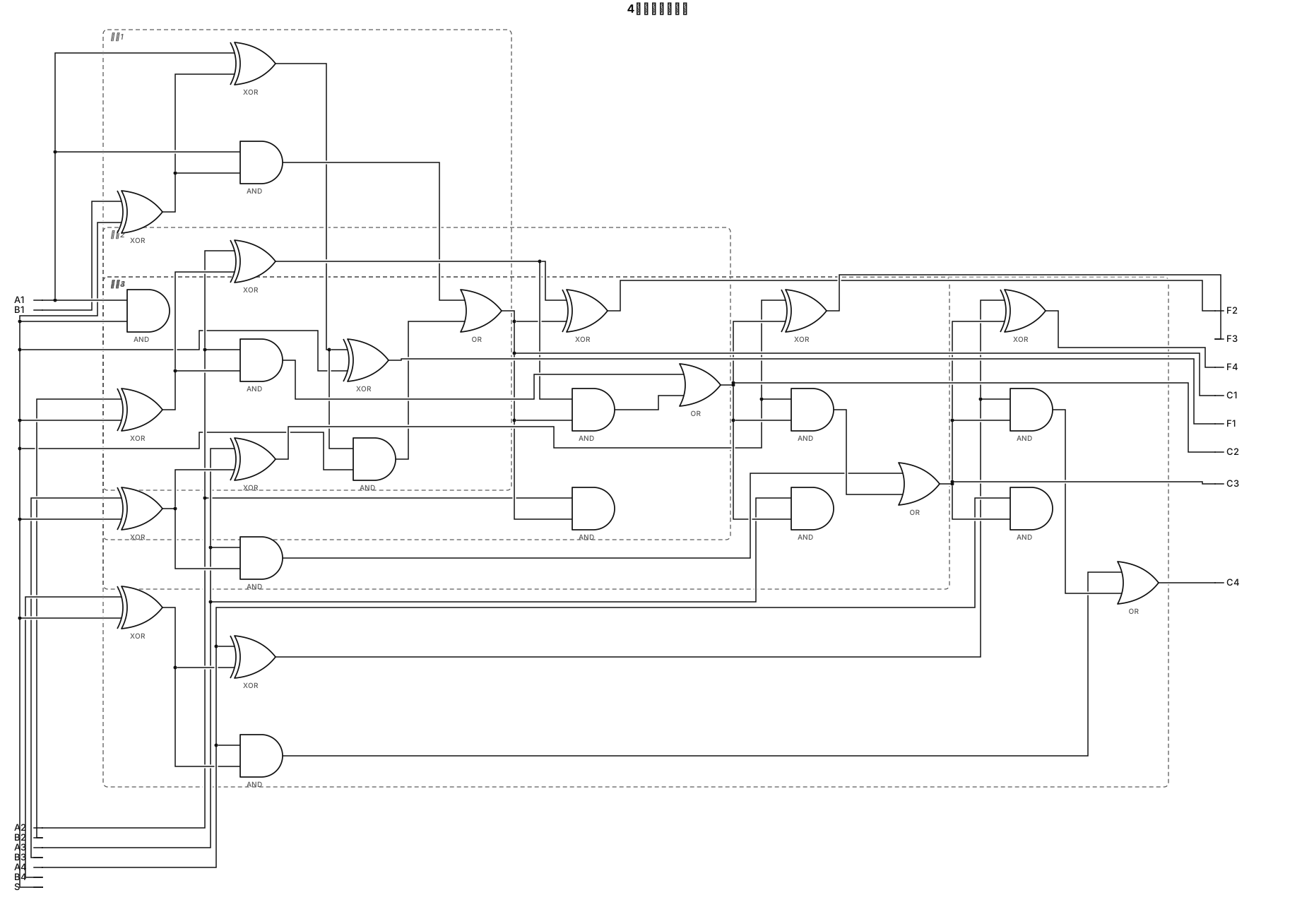
黑白线稿数字逻辑电路图,仅使用XOR异或门、AND与门、OR或门,不能使用全加器方块。 4个完全相同的可级联1位加减单元,从低位到高位依次为单元1、单元2、单元3、单元4。 每个单元输入:Ai, Bi, S, Cin;输出Fi, Cout。 每个单元内部:Bi和S送入XOR门,输出送入全加电路;全加电路由2个XOR、3个AND、1个OR组成。 所有单元共用同一个控制信号S。 单元1(最低位,A1,B1):Cin = S,输出F1,Cout=C1; 单元2(A2,B2):Cin接C1,输出F2,Cout=C2; 单元3(A3,B3):Cin接C2,输出F3,Cout=C3; 单元4(最高位,A4,B4):Cin接C3,输出F4,Cout=C4; 标注全部信号:A4,A3,A2,A1,B4,B3,B2,B1,S,F4,F3,F2,F1,C4,C3,C2,C1。线条规整,无多余装饰,计组作业图。
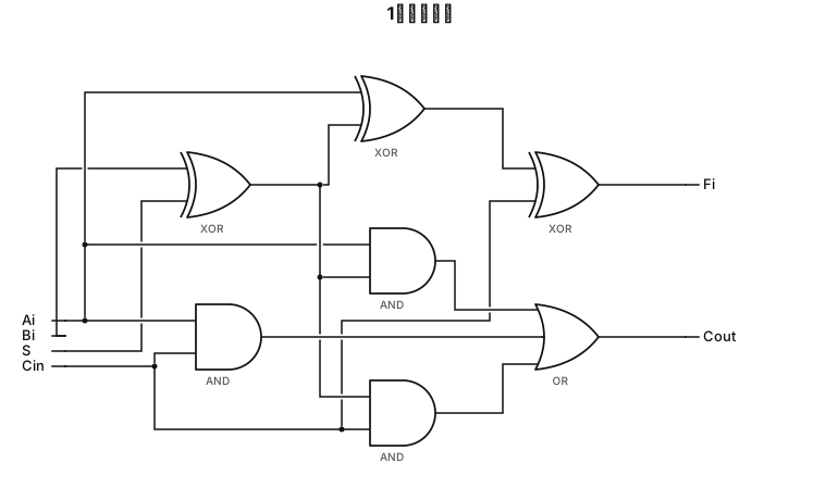
黑白线稿数字逻辑电路图,仅使用XOR异或门、AND与门、OR或门,不能使用全加器方块。 这是可级联的1位加减单元。 输入:Ai,Bi,S,Cin;输出:Fi,Cout。 第一个异或门:输入端接Bi和S,输出送到后面全加电路的一个输入。 全加电路部分: 第一个XOR门:输入Ai、上面异或门的输出; 第二个XOR门:输入上一个XOR的输出、Cin,输出本位Fi; 三个AND与门: 1. Ai 和 Bi⊕S的输出 2. Ai 和 Cin 3. Bi⊕S的输出 和 Cin 一个OR或门,接收三个与门的输出,输出Cout。 所有信号线标注:Ai, Bi, S, Cin, Fi, Cout。线条整齐,无多余装饰,计算机组成原理作业。
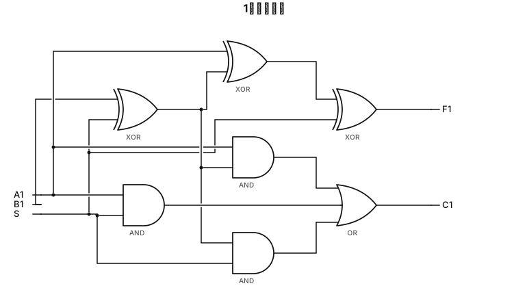
黑白线稿,1位加减法器,只用XOR异或门、AND与门、OR或门,不标注P1。 输入:A1,B1,控制信号S。 第一个异或门,两个输入端分别接B1和S;该异或门输出直接接到后面全加器的一个输入。 全加器另外两个输入:A1,以及C0=S。 全加器内部结构:第一个XOR接收A1和前面异或门的输出;第二个XOR接收该结果和C0,输出F1; 三个与门:A1和前面异或输出、A1和C0、前面异或输出和C0; 一个或门接收三个与门输出,输出C1。 所有引脚标注:A1、B1、S、F1、C1,线条简洁,无多余中间变量标签,计组作业图。
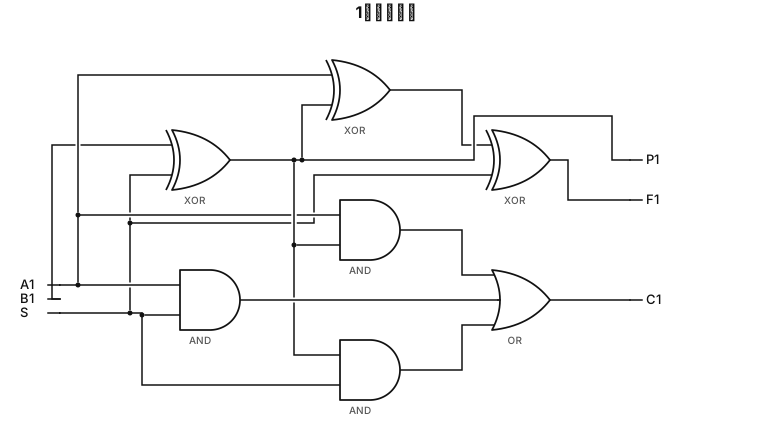
黑白线稿,1位加减法器,只用XOR、AND、OR门。 输入:A1,B1,控制S。 第一个异或门:输入B1和S,输出P1。 后面是展开的1位全加器:输入A1、P1、C0=S; 全加器内部:第一个XOR接收A1、P1;第二个XOR接收该结果和C0,输出F1; 三个与门分别是A1&P1,A1&C0,P1&C0; 一个或门接收三个与门输出,输出C1。 所有引脚标注A1,B1,S,P1,F1,C1,线条干净,作业用图。
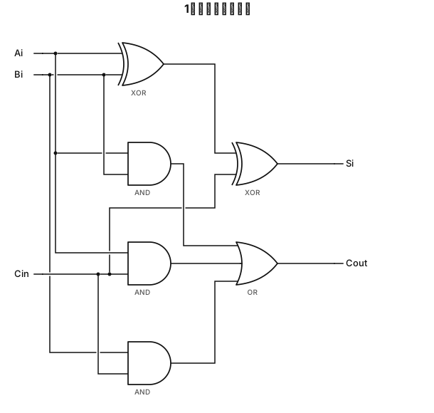
黑白线稿,1位全加器内部电路,只用XOR异或门、AND与门、OR或门。 输入:Ai,Bi,Cin;输出:Si,Cout。 第一个异或门:Ai、Bi输入,输出G1; 第二个异或门:G1、Cin输入,输出Si; 三个与门:Ai&Bi,Ai&Cin,Bi&Cin; 一个或门:接收三个与门的输出,输出Cout。 所有信号线标注名称,线条整齐,无多余装饰。
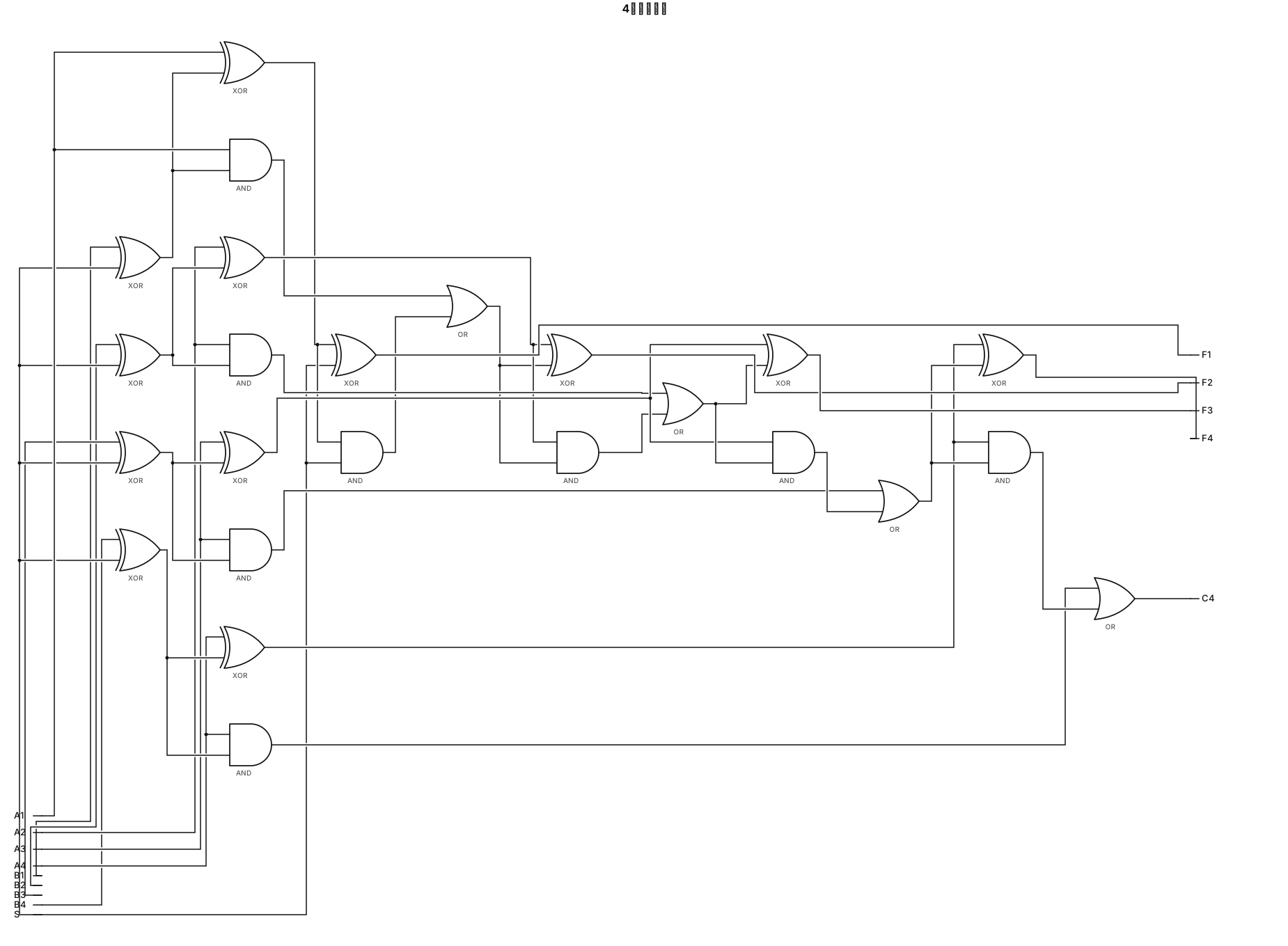
黑白线稿数字逻辑电路图,仅使用XOR异或门、AND与门、OR或门,不能使用全加器方块。 电路是4位加减法器,S=0加法,S=1减法。 输入信号:A4,A3,A2,A1,B4,B3,B2,B1,控制S。 B1~B4各自接入一个XOR门,XOR另一个输入端全部接S;XOR输出P1,P2,P3,P4。 共4组1位全加电路,每组全加电路由2个XOR、2个AND、1个OR构成。 第1组(最低位):输入A1、P1、C0=S,输出F1,进位C1; 第2组:输入A2、P2、C1,输出F2,进位C2; 第3组:输入A3、P3、C2,输出F3,进位C3; 第4组:输入A4、P4、C3,输出F4,进位C4; 所有信号线标注名称,线条规整,无多余装饰,计算机组成原理作业用图。
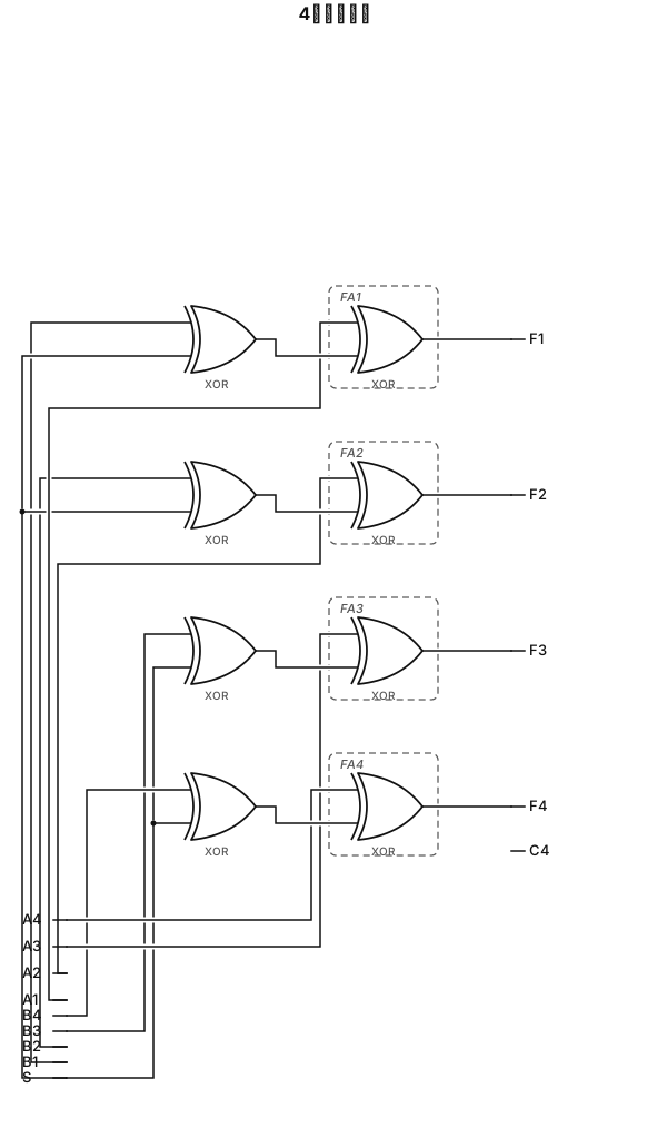
数字逻辑电路图,黑白线稿,标准逻辑门符号,4位加减法器,4个异或门,4个级联全加器FA1~FA4。 输入:A4,A3,A2,A1;B4,B3,B2,B1;控制信号S。 每个Bi接一个异或门的一个输入端,异或门另一个输入端全部接S;异或输出Pi送入对应全加器的B输入端。 Ai直接送入对应全加器A输入端。 最低位全加器FA1的进位输入C0 = S。 进位串行传递:FA1进位输出C1接到FA2进位输入,FA2进位C2接到FA3进位输入,FA3进位C3接到FA4进位输入。 输出:FA1输出F1,FA2输出F2,FA3输出F3,FA4输出F4,FA4进位输出C4。 所有引脚标注文字,线条清晰,无多余装饰,适合计算机组成原理作业。
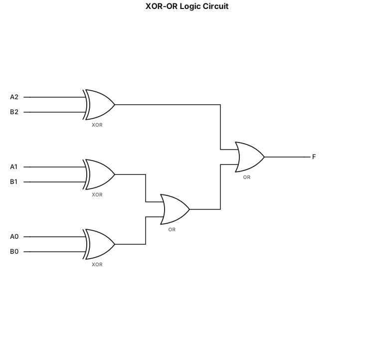
Draw a digital logic circuit schematic using IEEE standard symbols. Inputs: A2, B2, A1, B1, A0, B0. Gate 1: XOR gate with inputs A2 and B2 yielding output F2. Gate 2: XOR gate with inputs A1 and B1 yielding output F1. Gate 3: XOR gate with inputs A0 and B0 yielding output F0. Gate 4: 2-input OR gate taking F1 and F0 as inputs to yield F10. Gate 5: 2-input OR gate taking F2 and F10 as inputs to yield final output F.
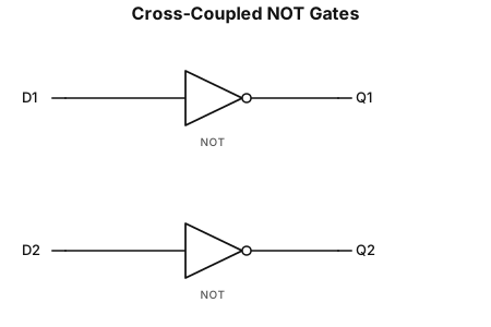
A logic gate circuit 2 inputs D1 D2 connected with 2 different not gates with each one one output Q1 Q2. the output of D1 goes as input of D2 and viceversa
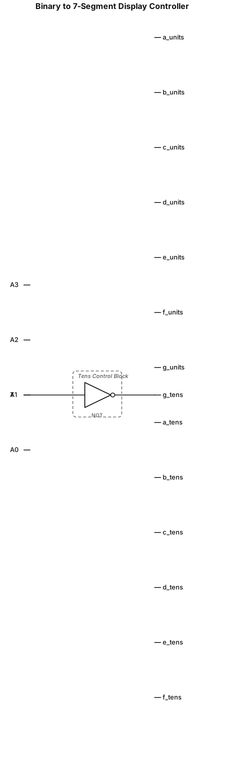
Inputs: 4 lines labeled A3, A2, A1, A0 on the left. Block 1 ('Binary to BCD Converter'): Uses AND, OR, and NOT gates to output a Tens bit (T) and four Units bits (U3, U2, U1, U0). Block 2 ('Units 7-Segment Decoder'): Takes U3-U0. Uses shared AND gates feeding into OR gates. Outputs a_units through g_units. Block 3 ('Tens Control Block'): Takes T. Uses NOT gates and fixed VCC/GND connections. Outputs a_tens through g_tens. Layout: Left-to-right flow, straight orthogonal lines, standard logic gate symbols (ANSI/IEEE), and clear text labels."
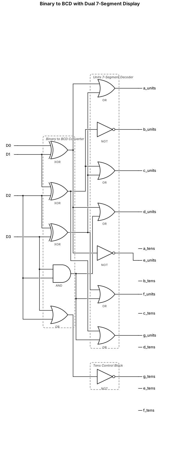
Design a circuit that takes a number from 0 to 15 and represents it using two 7 segment displays, the flow goes like this Input-> convertion from binary to BCD ->7segment decoder for the units and a control block for the decimal
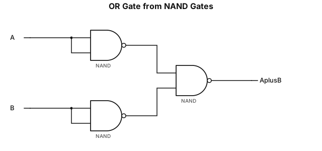
OR Gate Implementation:Show two inputs, $A$ and $B$.Feed input $A$ into a NAND-based NOT gate to get $\overline{A}$, and input $B$ into another NAND-based NOT gate to get $\overline{B}$.Feed both $\overline{A}$ and $\overline{B}$ into a third NAND gate.Label the final output as $A + B$.
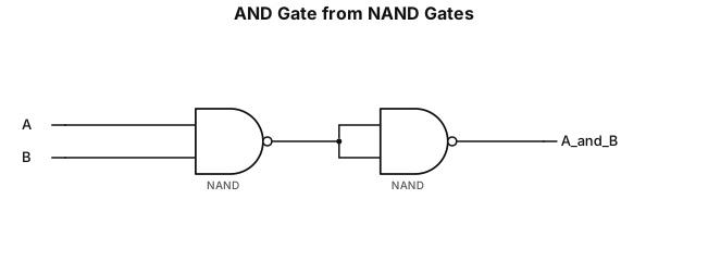
AND Gate Implementation:Show a 2-input NAND gate with inputs $A$ and $B$, producing an intermediate output $\overline{A \cdot B}$.Connect this output into a second NAND gate configured as a NOT gate (both inputs tied together).Label the final output as $A \cdot B$.
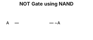
NOT Gate Implementation:Show a single 2-input NAND gate where both inputs ($A$) are tied together into a single input line.Label the input as $A$ and the output as $\overline{A}$.
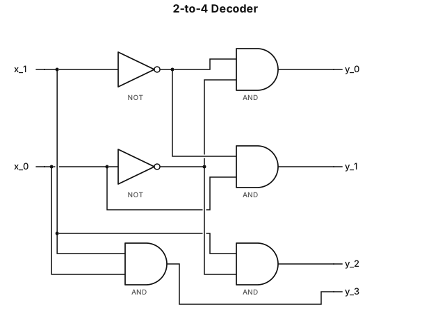
Task: Draw a circuit diagram of a 2-to-4 decoder based on a network of logic gates. Operation and logic: Inputs: x_1 and x_0 (a 2-bit binary number). Outputs: y_3, y_2, y_1, y_0 (one-hot encoding). Boolean equations: y_0 = \bar{x}_1 \bar{x}_0, y_1 = \bar{x}_1 x_0, y_2 = x_1 \bar{x}_0, y_3 = x_1 x_0. Diagram construction instructions: Place two input lines, x_1 and x_0, on the left side. Add NOT gates (inverters) to the input lines to obtain the negated signals \bar{x}_1 and \bar{x}_0. On the right side, place four 2-input AND gates (or AND gates with inverted inputs—indicated by "bubbles"). Connect the inputs to the AND gates as follows: First AND gate: inputs \bar{x}_1 and \bar{x}_0 \rightarrow output y_0. Second AND gate: inputs \bar{x}_1 and x_0 \rightarrow output y_1. Third AND gate: inputs x_1 and \bar{x}_0 \rightarrow output y_2. Fourth AND gate: inputs x_1 and x_0 \rightarrow output y_3. Label the inputs of all gates and... outputs clearly labeled (x_1, x_0, y_0, y_1, y_2, y_3). Draw the diagram with a clear white background and black lines. and can you make the x stand sidebyside and the y stand sidebyside
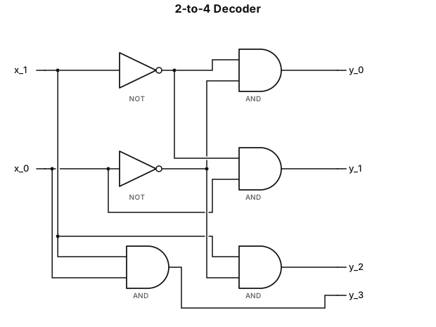
Task: Draw a circuit diagram of a 2-to-4 decoder based on a network of logic gates. Operation and logic: Inputs: x_1 and x_0 (a 2-bit binary number). Outputs: y_3, y_2, y_1, y_0 (one-hot encoding). Boolean equations: y_0 = \bar{x}_1 \bar{x}_0, y_1 = \bar{x}_1 x_0, y_2 = x_1 \bar{x}_0, y_3 = x_1 x_0. Diagram construction instructions: Place two input lines, x_1 and x_0, on the left side. Add NOT gates (inverters) to the input lines to obtain the negated signals \bar{x}_1 and \bar{x}_0. On the right side, place four 2-input AND gates (or AND gates with inverted inputs—indicated by "bubbles"). Connect the inputs to the AND gates as follows: First AND gate: inputs \bar{x}_1 and \bar{x}_0 \rightarrow output y_0. Second AND gate: inputs \bar{x}_1 and x_0 \rightarrow output y_1. Third AND gate: inputs x_1 and \bar{x}_0 \rightarrow output y_2. Fourth AND gate: inputs x_1 and x_0 \rightarrow output y_3. Label the inputs of all gates and... outputs clearly labeled (x_1, x_0, y_0, y_1, y_2, y_3). Draw the diagram with a clear white background and black lines.
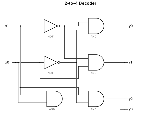
Task: Draw a circuit diagram of a 2-to-4 decoder based on a network of logic gates. Operation and logic: Inputs: $x_1$ and $x_0$ (a 2-bit binary number). Outputs: $y_3, y_2, y_1, y_0$ (one-hot encoding). Boolean equations: $y_0 = \bar{x}_1 \bar{x}_0$, $y_1 = \bar{x}_1 x_0$, $y_2 = x_1 \bar{x}_0$, $y_3 = x_1 x_0$. Diagram construction instructions: Place two input lines, $x_1$ and $x_0$, on the left side. Add NOT gates (inverters) to the input lines to obtain the negated signals $\bar{x}_1$ and $\bar{x}_0$. On the right side, place four 2-input AND gates (or AND gates with inverted inputs—indicated by "bubbles"). Connect the inputs to the AND gates as follows: First AND gate: inputs $\bar{x}_1$ and $\bar{x}_0 \rightarrow$ output $y_0$. Second AND gate: inputs $\bar{x}_1$ and $x_0 \rightarrow$ output $y_1$. Third AND gate: inputs $x_1$ and $\bar{x}_0 \rightarrow$ output $y_2$. Fourth AND gate: inputs $x_1$ and $x_0 \rightarrow$ output $y_3$. Label the inputs of all gates and... outputs clearly labeled ($x_1, x_0, y_0, y_1, y_2, y_3$). Draw the diagram with a clear white background and black lines.
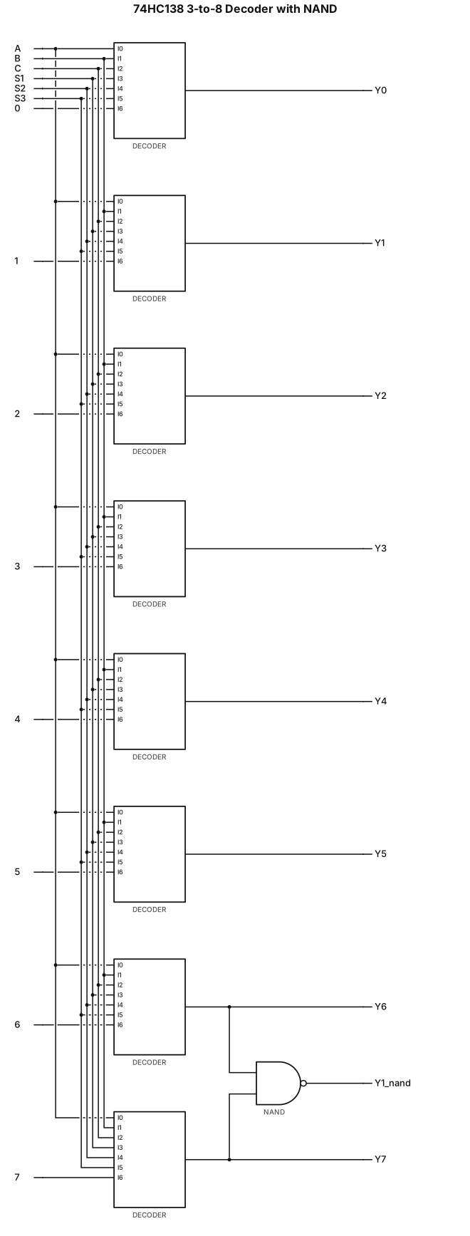
One single 74HC138 3-to-8 decoder. A2,A1,A0 = A,B,C. S1=1, S2=0, S3=0. Only one 2-input NAND gate, inputs connect to Y6 and Y7 of this decoder, output Y1. Standard IEEE logic symbols, clean wires, exam style.