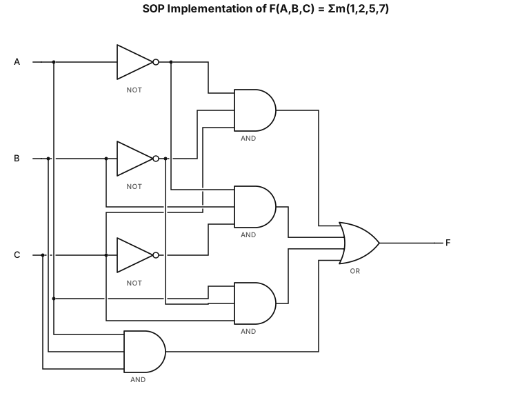
2.1 SOP Implementation Using Basic Logic Gates Given: F(A,B,C) = Σm(1,2,5,7)
NODE ARCHIVE · REAL DIAGRAM BRIEFS
Diagram Examples from Real Visitor Prompts
Browse eligible diagrams shared by FreeDiagram visitors, inspect the exact prompts, and build your own version.
Browse 3260 real creationsCOMMUNITY OUTPUTS · EXACT PROMPTS
Boolean Expression To Logic Circuit
Showing 49–72 of 98. No stock examples or system defaults. Choose a tool, study a real result, then reopen its prompt as your starting point.
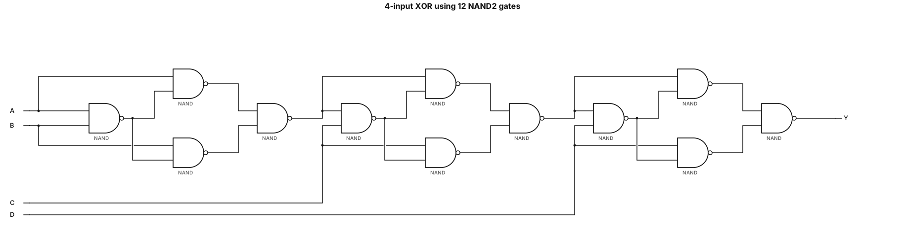
Draw a 4-input XOR logic circuit using ONLY 2-input NAND gates. Boolean function: Y = A XOR B XOR C XOR D STRICT REQUIREMENTS: - Use exactly 12 NAND2 gates. - Only inputs A, B, C, D are available. - No complementary inputs. - Do NOT use XOR, XNOR, AND, OR, NOT, or NAND3 gates. - Do NOT simplify or change the gate structure. Use these exact connections: Stage 1: N1 = NAND(A, B) N2 = NAND(A, N1) N3 = NAND(B, N1) X1 = NAND(N2, N3) Stage 2: N4 = NAND(X1, C) N5 = NAND(X1, N4) N6 = NAND(C, N4) X2 = NAND(N5, N6) Stage 3: N7 = NAND(X2, D) N8 = NAND(X2, N7) N9 = NAND(D, N7) Y = NAND(N8, N9) Draw all 12 NAND2 gates with labeled wires and inputs, from left to right. Total NAND2 gates = 12. Each NAND2 has 2 NMOS. Total NMOS = 24.
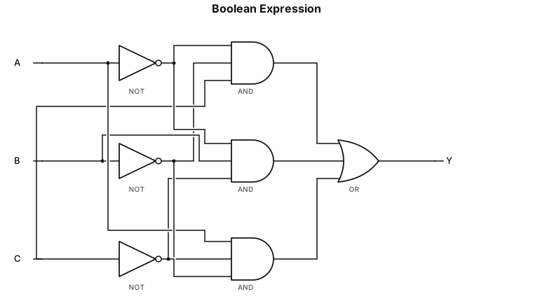
Y = (!A & !B & C) | (!A & B & !C) | (A & !B & !C)
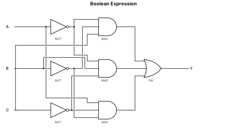
Y = Ā B̄ C + Ā B C̄ + A B̄ C̄
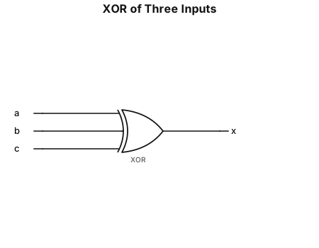
\[ \boxed{x=a\oplus b\oplus c} \]
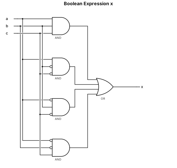
\[ x=abc+a\bar b\bar c+\bar ab\bar c+\bar a\bar bc \]
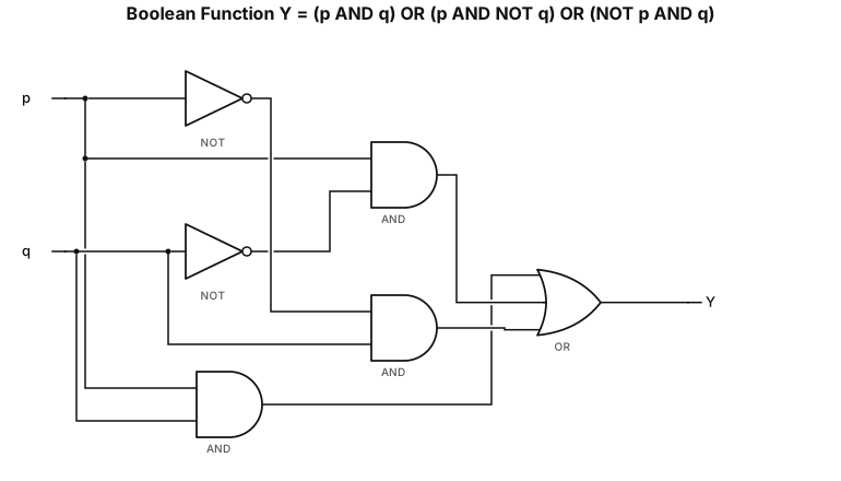
Draw a clean, accurate digital logic gate circuit diagram for this Boolean function: Y = (p AND q) OR (p AND NOT q) OR (NOT p AND q) Requirements: 1. Use exactly three 2-input AND gates, two NOT gates, and one 3-input OR gate. 2. AND gate 1 inputs: p and q. 3. AND gate 2 inputs: p and NOT q. 4. AND gate 3 inputs: NOT p and q. 5. Connect the three AND gate outputs to the three inputs of the final OR gate. 6. Label every input, intermediate output, and final output Y. 7. Arrange the circuit from left to right with neat, non-crossing wires. 8. Use standard logic gate symbols on a plain white background. 9. Do not simplify the Boolean expression. 10. Generate the actual circuit diagram, not a text explanation.
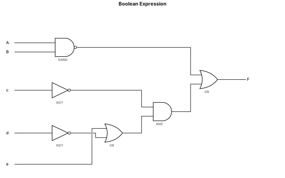
F = (A B)' + c' . (e + d')
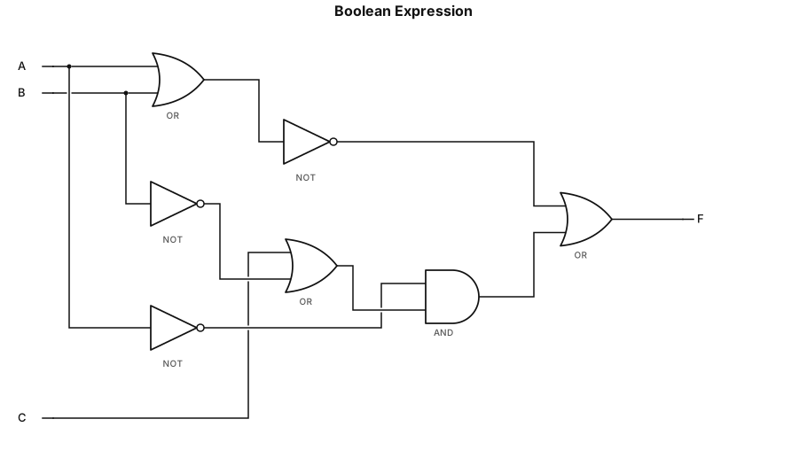
F = (A + B)' + A̅ . (C + B̅)
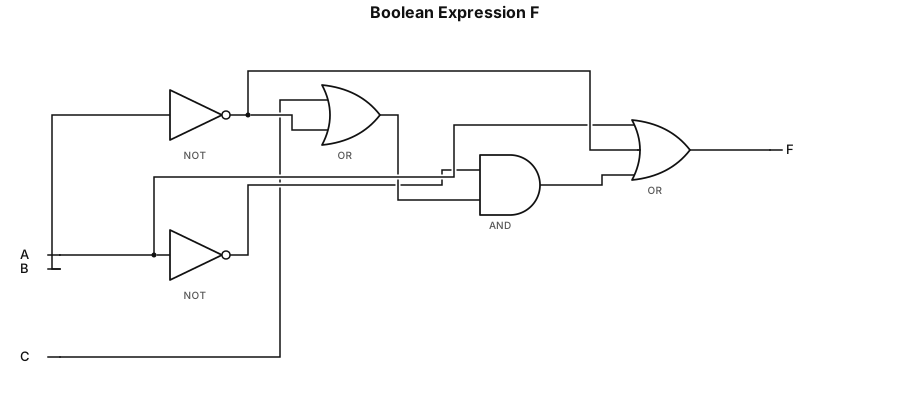
F = A + B̅ + A̅ . (C + B̅)
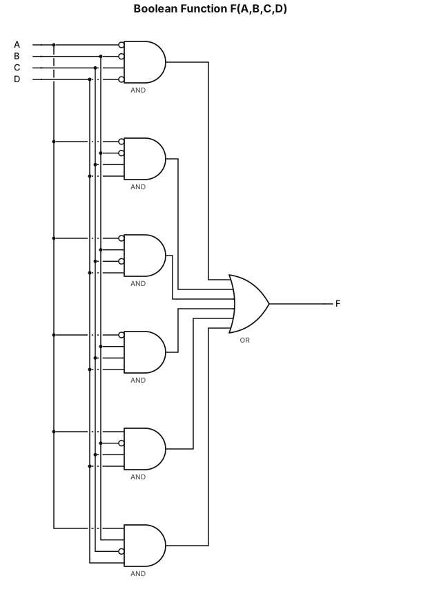
F(A ,B ,C ,D) = A'B'CD' + A'B'CD + A'BC'D + A'BCD + AB'CD + ABC'D
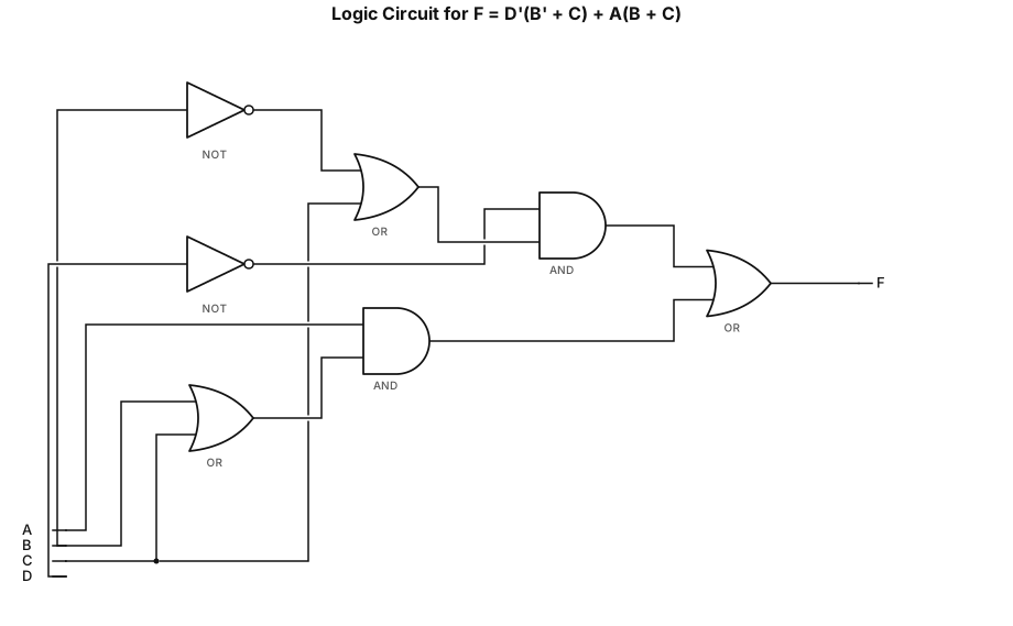
Draw the logic circuit diagram for F = D'(B' + C) + A(B + C), strictly using 2 inputs only
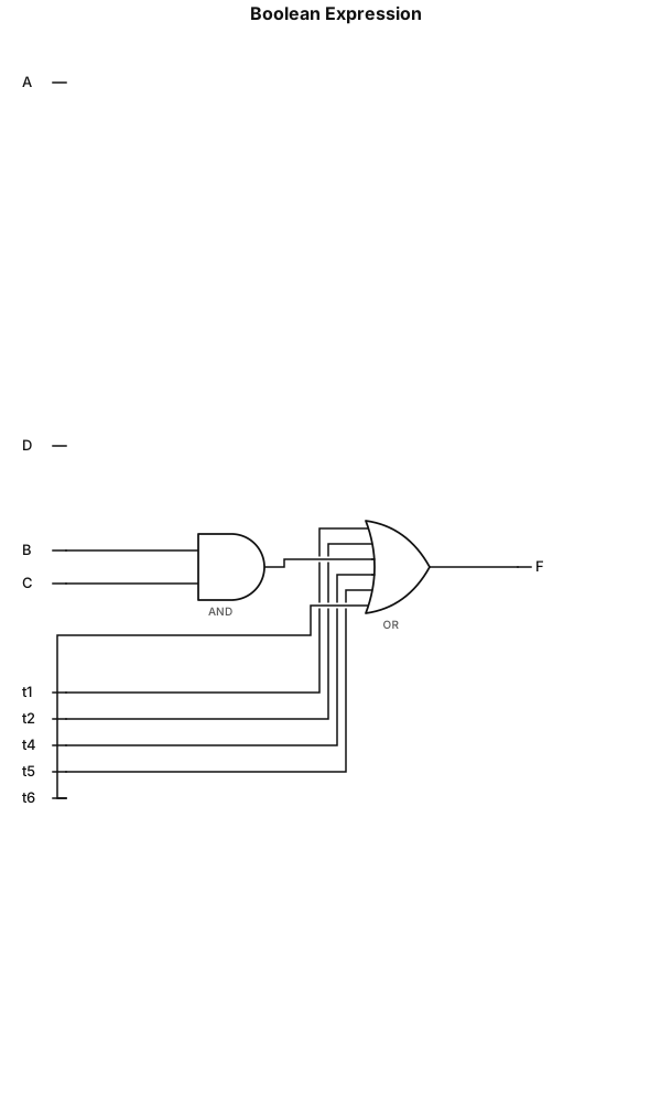
B'·D' + A'·C + B·C + A·D' + A'·B·D + A·B'·C'
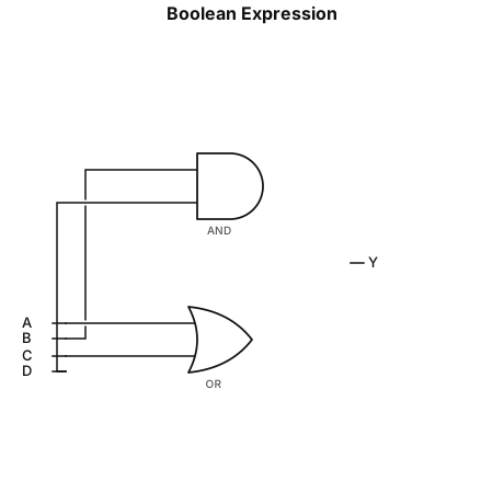
A + C + B·D + B'·D'
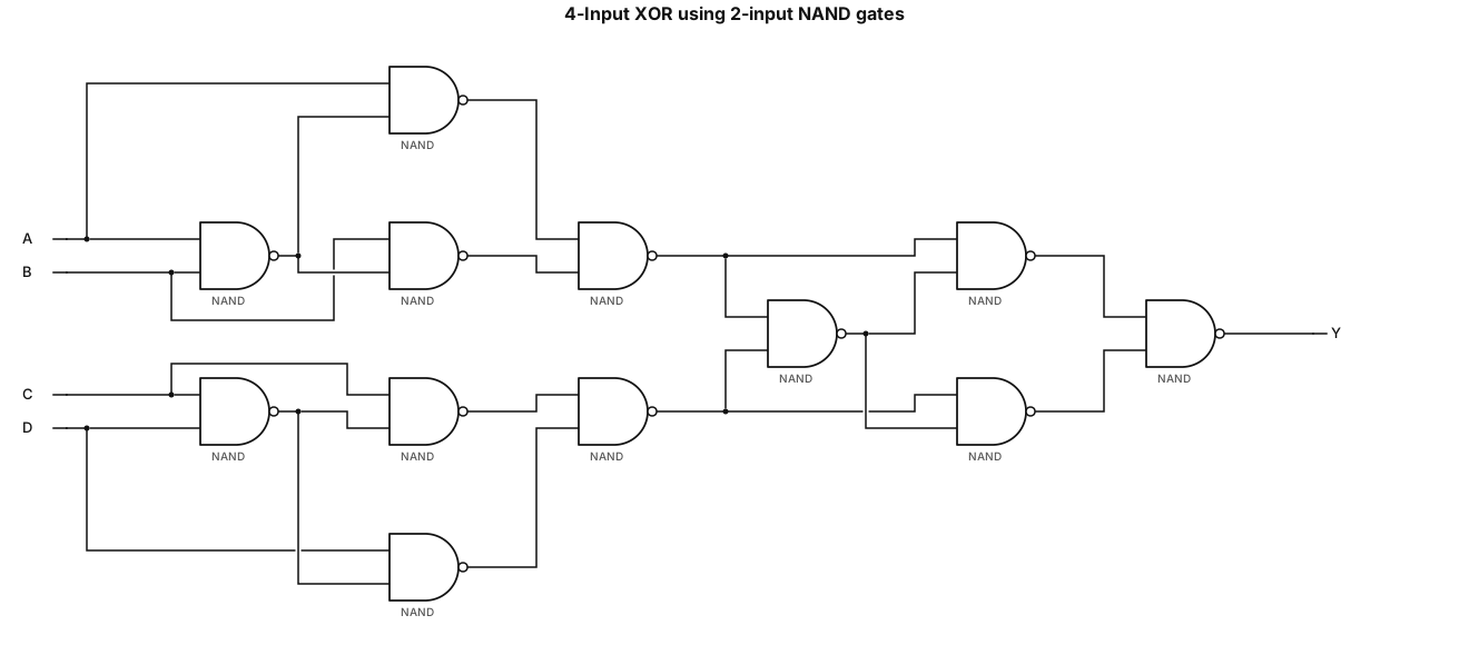
Draw a gate-level schematic of Y = A XOR B XOR C XOR D using only 2-input NAND gates.
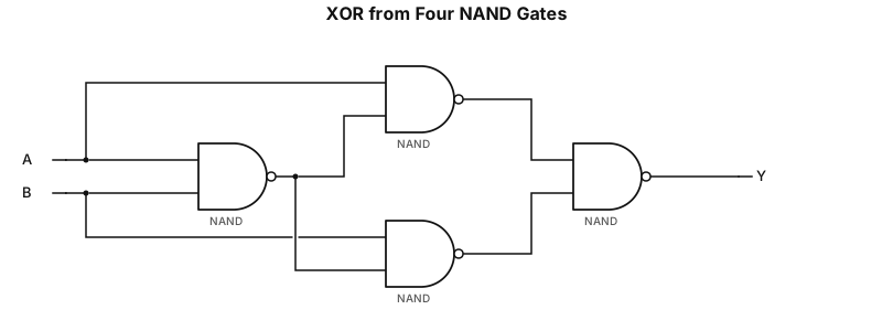
Draw a transistor-free gate-level schematic of Y = A XOR B using exactly four 2-input NAND gates. Show all connections. Do not use XOR gate symbols
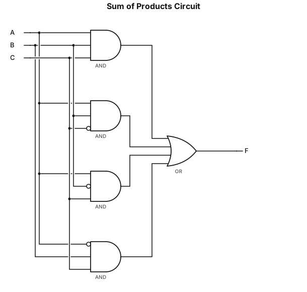
Draw an AND gate for each term (raw in the truth table) with a 1 in the result column Wire the AND gates to the appropriate inputs Feed the output of all the AND gates into an OR gate
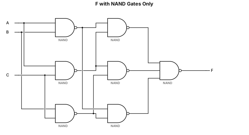
F = A'B'C' + ABC' + AB'C + A'BC NAND gates only
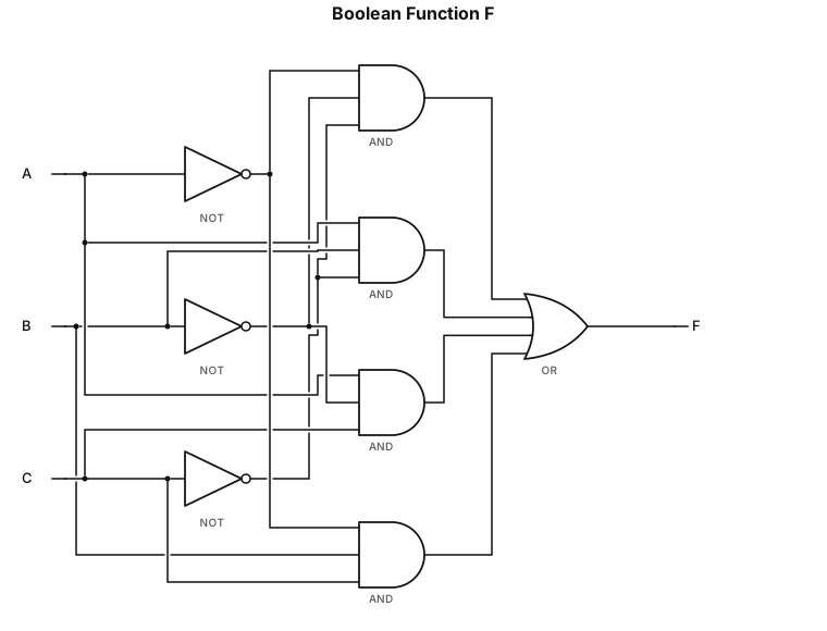
F = A'B'C' + ABC' + AB'C + A'BC
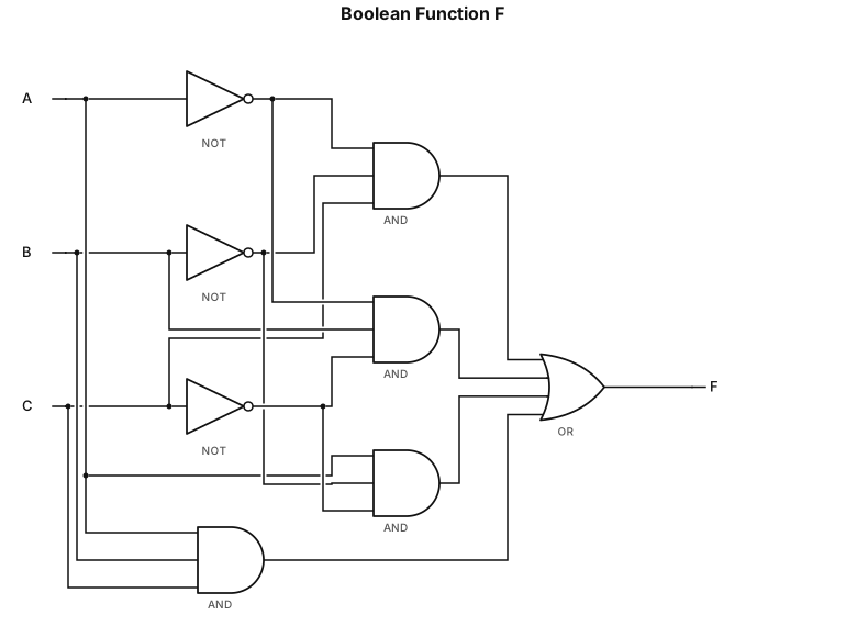
F = A'B'C + A'BC' + AB'C' + ABC
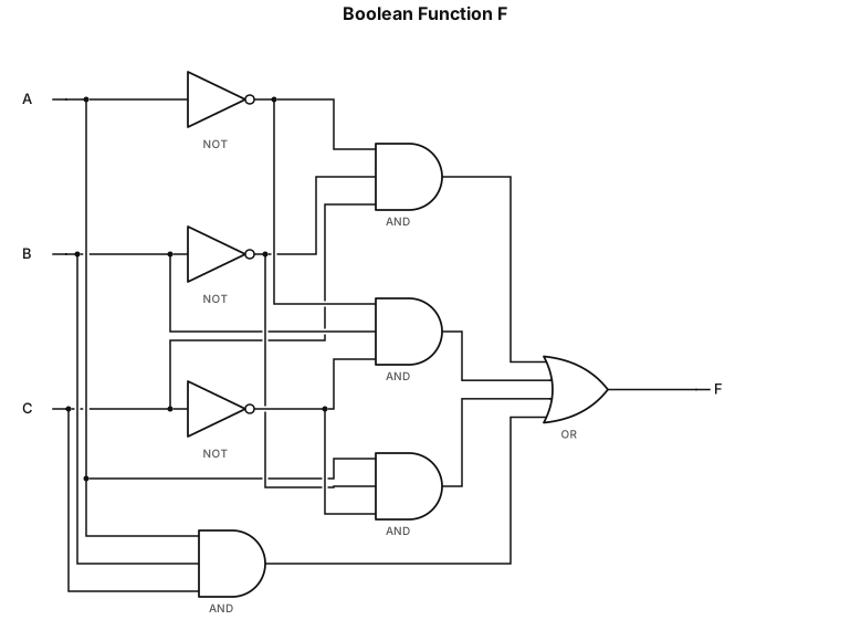
\[ F=\overline A\overline B C +\overline A B\overline C +A\overline B\overline C +ABC \]
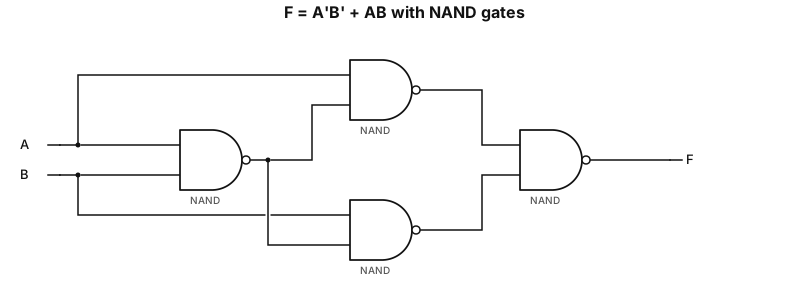
F = A'B' + AB implemented with NAND gates only
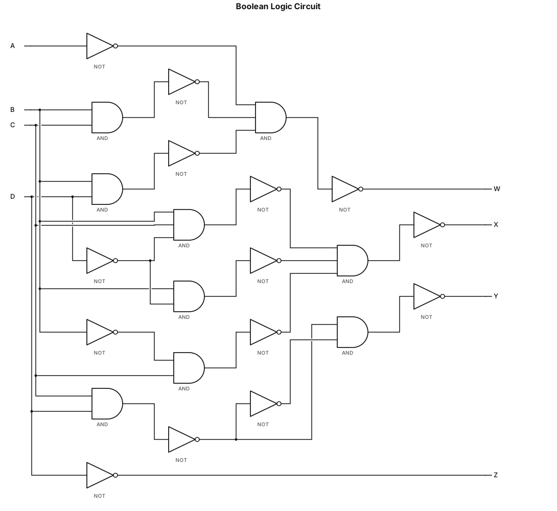
W = NOT ((NOT A) AND (NOT (B AND C)) AND (NOT (B AND D))) X = NOT ((NOT (B AND C AND (NOT D))) AND (NOT (B AND (NOT D))) AND (NOT ((NOT B) AND C))) Y = NOT ((NOT (C AND D)) AND (NOT (NOT (C AND D)))) Z = NOT D
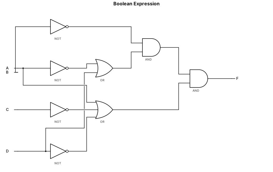
F = B′ · (A′ + D) · (A + C′ + D′)