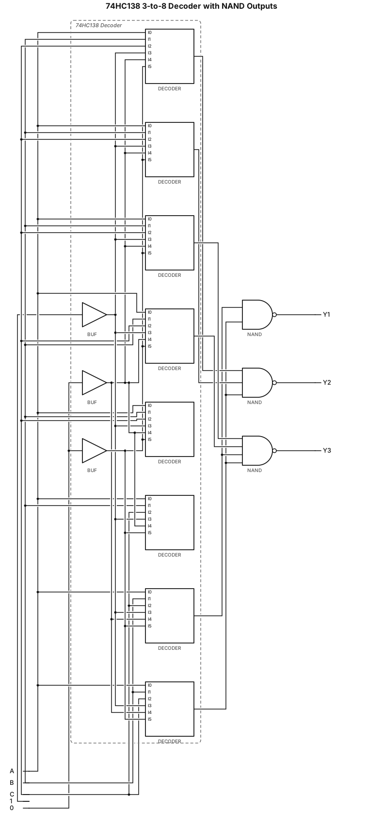
Digital logic circuit, ONLY ONE 74HC138 3-to-8 decoder chip. Address pins A2,A1,A0 connect to A,B,C. Enable S1=1, S2=0, S3=0. There are three NAND gates connected to the output of this single decoder: 2-input NAND: inputs Y6,Y7, output Y1 3-input NAND: inputs Y0,Y1,Y7, output Y2 4-input NAND: inputs Y2,Y3,Y6,Y7, output Y3 Standard IEEE symbols, white background, clean orthogonal wires, label all pins, for digital electronics exam
NODE ARCHIVE · REAL DIAGRAM BRIEFS
Diagram Examples from Real Visitor Prompts
Browse eligible diagrams shared by FreeDiagram visitors, inspect the exact prompts, and build your own version.
Browse 3261 real creationsCOMMUNITY OUTPUTS · EXACT PROMPTS
Logic Gate
Showing 49–72 of 288. No stock examples or system defaults. Choose a tool, study a real result, then reopen its prompt as your starting point.
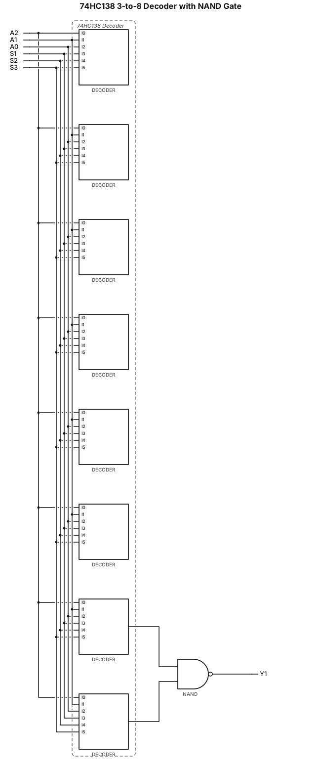
Digital logic circuit with 74HC138 3-to-8 decoder. Address pins A2,A1,A0 connect to A,B,C. Enable S1=1, S2=0, S3=0. 2-input NAND gate, inputs Y6,Y7, output Y1. Standard IEEE symbols, white background, clean orthogonal wires, label all pins, for digital electronics exam
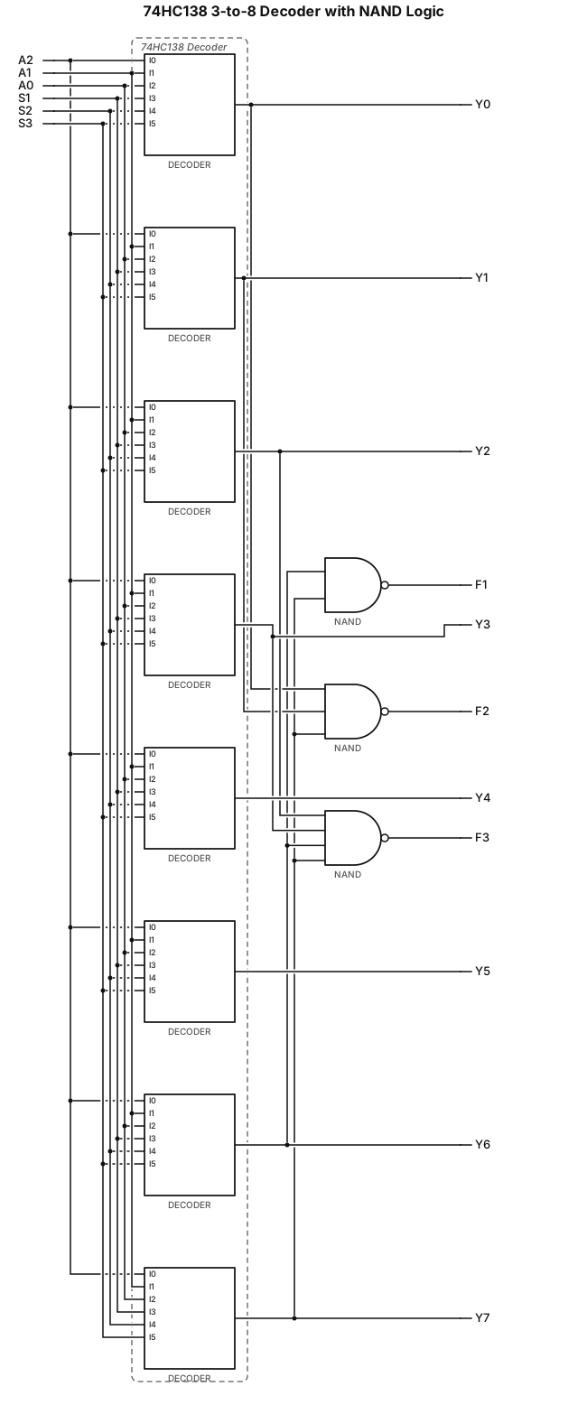
Digital logic circuit with 74HC138 3-to-8 decoder. Address pins A2,A1,A0 connect to A,B,C. Enable S1=1, S2=0, S3=0. Three NAND gates: 2-input NAND: inputs Y6,Y7, output Y1 3-input NAND: inputs Y0,Y1,Y7, output Y2 4-input NAND: inputs Y2,Y3,Y6,Y7, output Y3 Standard IEEE symbols, white background, clean orthogonal wires, label all pins, for digital electronics exam
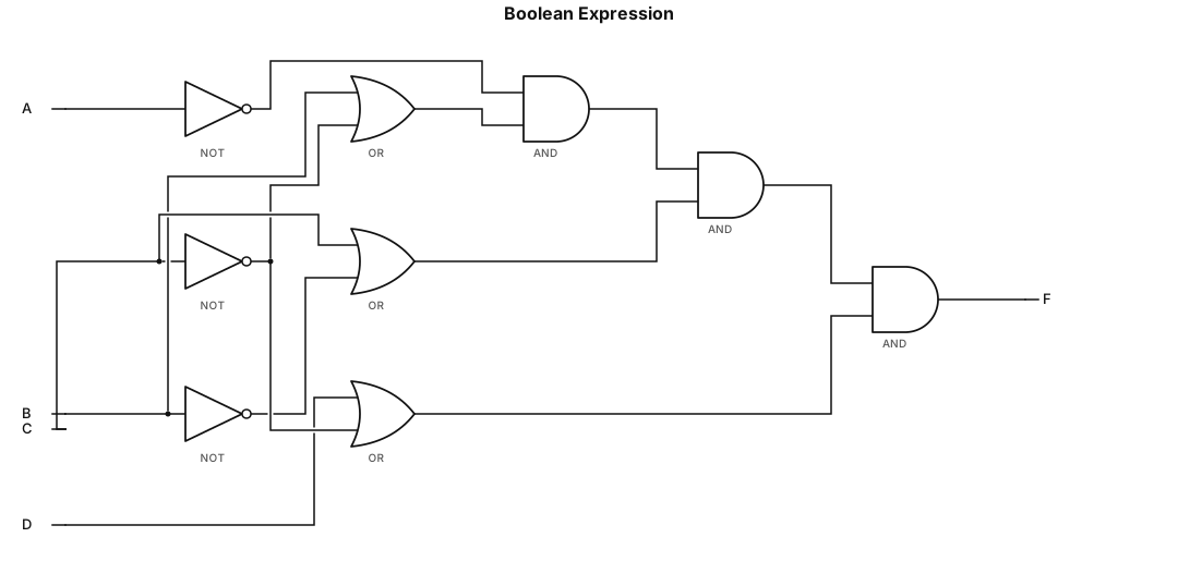
A'(B + C')(C + B')(D + C')
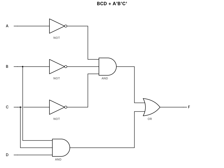
(BCD) + (A'B'C')
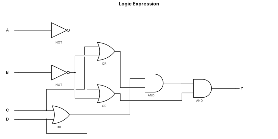
A'(C + D)(C + B')(D + B')
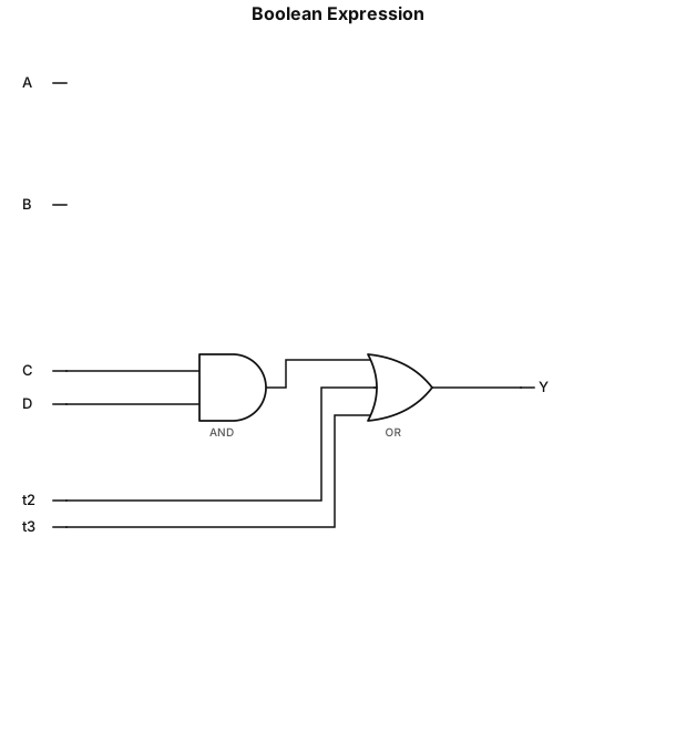
(CD) + (CB') + (DA'B')
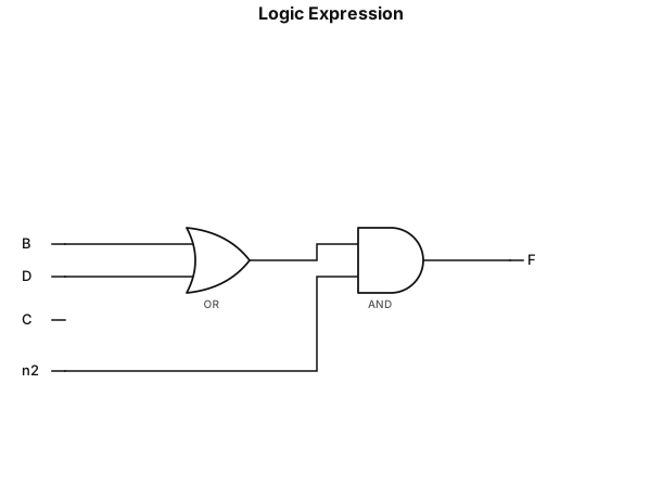
(B + D)(D + C')
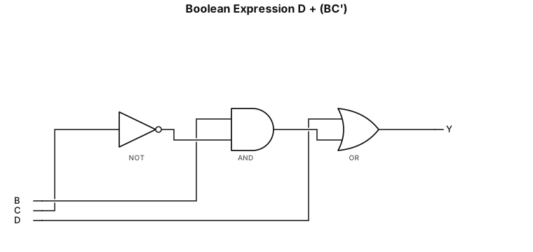
D + (BC')
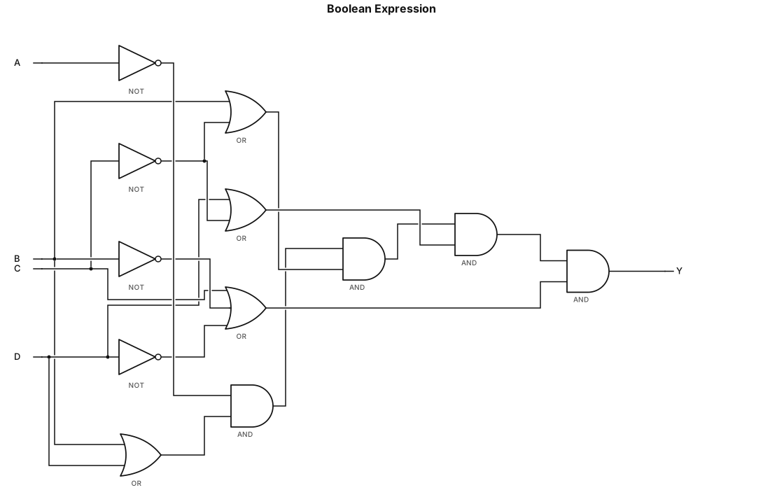
A'(B + D)(B + C')(D + C')(C + B' + D')
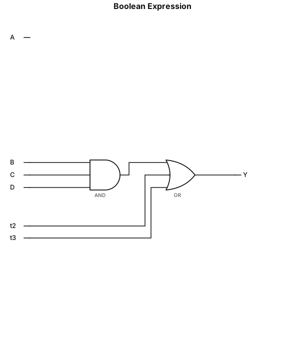
(BCD) + (BC'D') + (DA'B'C')
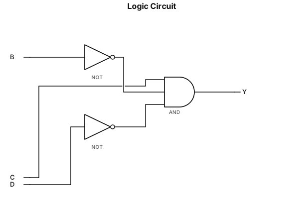
CB'D'
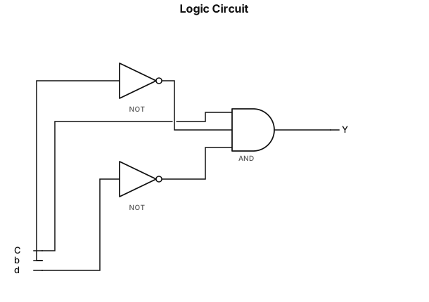
Cb'd'
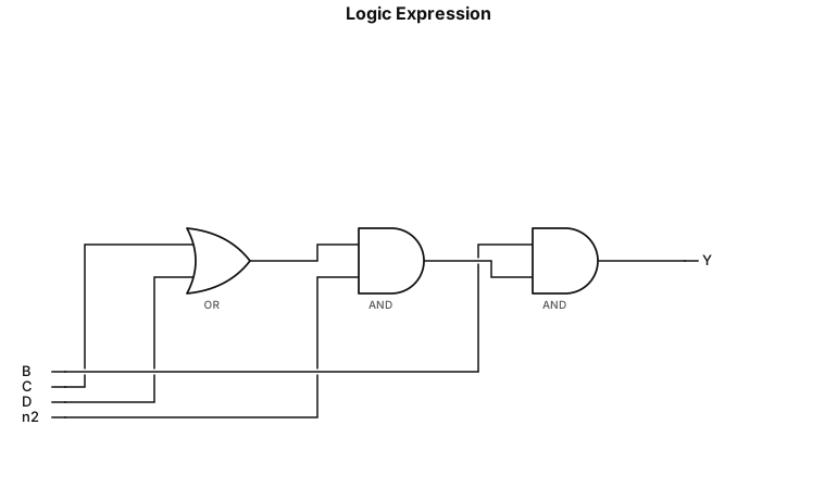
B(C + D)(C'+ D')
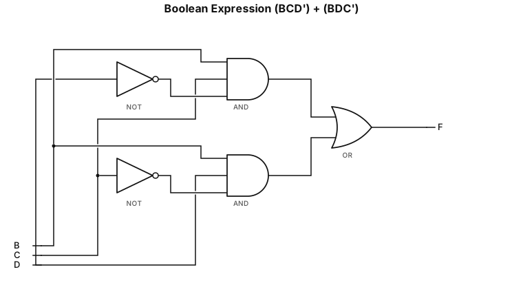
(BCD') + (BDC')
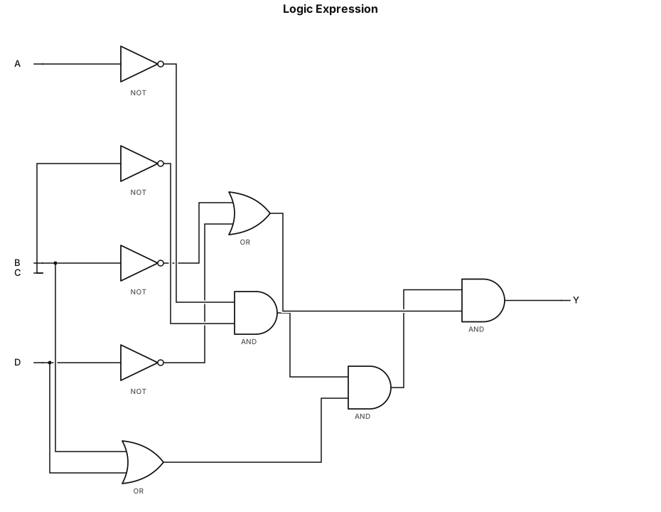
A'C'(B + D)(B' + D')
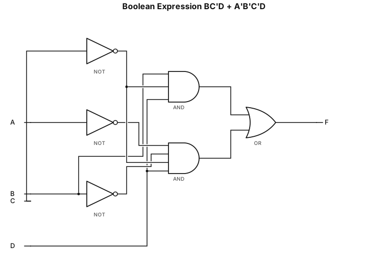
BC'D+A'B'C'D
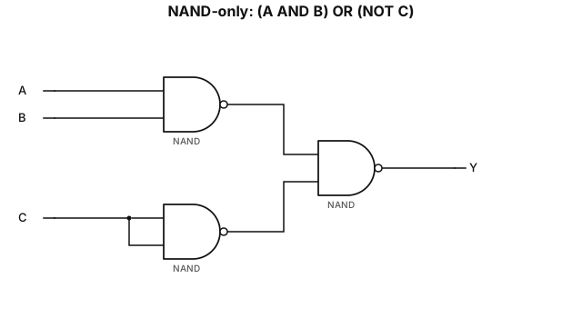
NAND-only implementation of the expression (A AND B) OR (NOT C)
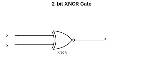
A logic gate circuit for a 2-bit XNOR gate with inputs x, y. and output f.
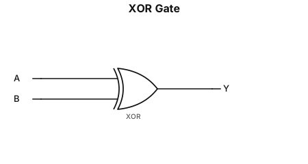
A XOR B
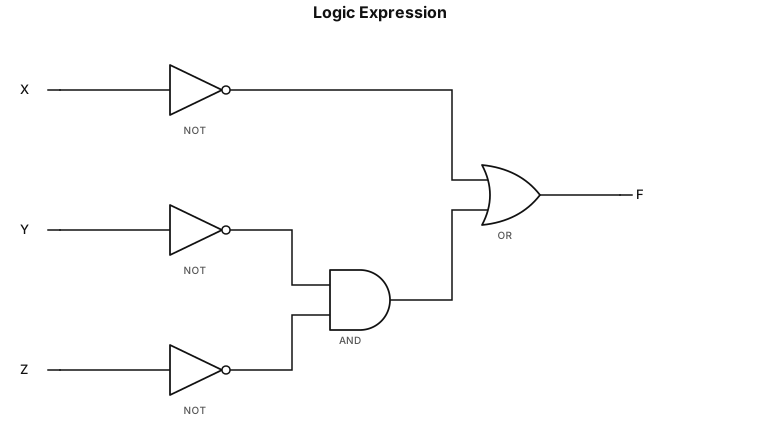
X'+Y'Z'
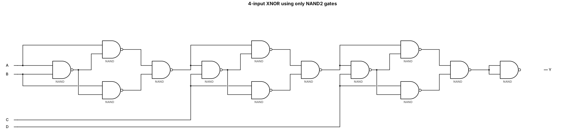
Draw a complete 4-input XNOR gate-level schematic using ONLY 2-input NAND gates. Final Boolean function: Y = NOT(A XOR B XOR C XOR D) Exactly four primary inputs: A, B, C, D. Use exactly 13 NAND2 gates. Follow this exact netlist: N1 = NAND(A, B) N2 = NAND(A, N1) N3 = NAND(B, N1) N4 = NAND(N2, N3) N5 = NAND(N4, C) N6 = NAND(N4, N5) N7 = NAND(C, N5) N8 = NAND(N6, N7) N9 = NAND(N8, D) N10 = NAND(N8, N9) N11 = NAND(D, N9) N12 = NAND(N10, N11) N13 = NAND(N12, N12) Y = N13 Drawing requirements: - Use only NAND2 symbols (AND-shaped gate with an output inversion bubble). - Do not use XOR, XNOR, NOR, OR, AND or separate inverter symbols. - Show all 13 gates individually. - Label gates N1 through N13. - Arrange the circuit in three stages followed by the final NAND2 inverter. - Connect every wire exactly according to the netlist. - Explicitly connect N13 output to Y. - Avoid overlapping wires and ambiguous connections. - Use a clean black-and-white textbook-style gate-level schematic. - Verify all 16 input combinations. - Do not change the gate count or Boolean functions.
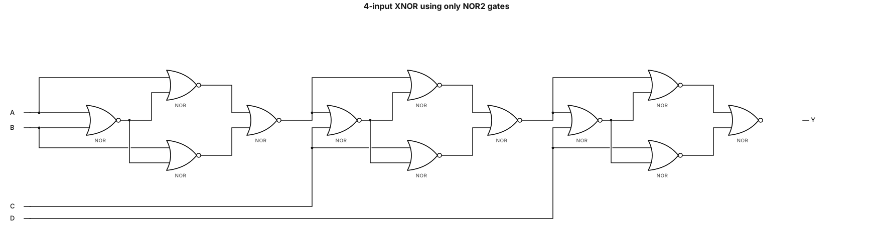
Draw a complete gate-level logic circuit for a 4-input XNOR (XNOR4) using ONLY 2-input NOR gates. Boolean function: Y = NOT(A XOR B XOR C XOR D) Requirements: - Exactly four primary inputs: A, B, C, D. - Use ONLY NOR2 gates. - Do NOT use XOR, XNOR, AND, OR, NAND, or NOT gate symbols. - No complemented primary inputs are available. - Draw exactly 12 NOR2 gates. - Show every intermediate signal and connection. - Arrange the circuit from left to right in three stages. - Do not simplify or replace any NOR2 network with XOR/XNOR symbols. Implement the following exact gate-level netlist: STAGE 1: 4 NOR2 gates N1 = NOR(A, B) N2 = NOR(A, N1) N3 = NOR(B, N1) N4 = NOR(N2, N3) STAGE 2: 4 NOR2 gates N5 = NOR(N4, C) N6 = NOR(N4, N5) N7 = NOR(C, N5) N8 = NOR(N6, N7) STAGE 3: 4 NOR2 gates N9 = NOR(N8, D) N10 = NOR(N8, N9) N11 = NOR(D, N9) N12 = NOR(N10, N11) FINAL OUTPUT: Y = N12 Show exactly 12 individual NOR2 symbols labeled N1 through N12. All wires must follow the exact netlist above. Use a clean black-and-white engineering textbook schematic with clearly labeled inputs, intermediate nodes, and output Y. Verify that Y=1 when the number of HIGH inputs among A, B, C, D is even. Do not optimize or change the specified gate connections.
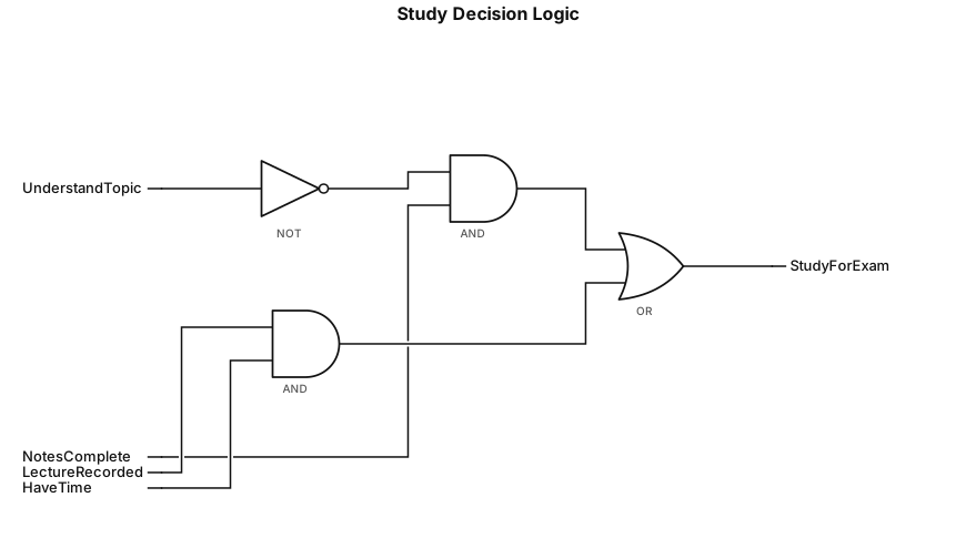
If I do not understand the topic and the notes are complete, or if the lecture is recorded and I have time, then I will study for the exam.