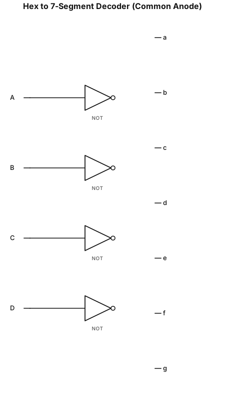
A four binary input combinational circuit that makes a hex-to-seven segment output with a common anode 7 segment
NODE ARCHIVE · REAL DIAGRAM BRIEFS
Diagram Examples from Real Visitor Prompts
Browse eligible diagrams shared by FreeDiagram visitors, inspect the exact prompts, and build your own version.
Browse 3261 real creationsCOMMUNITY OUTPUTS · EXACT PROMPTS
Logic Gate
Showing 97–120 of 288. No stock examples or system defaults. Choose a tool, study a real result, then reopen its prompt as your starting point.
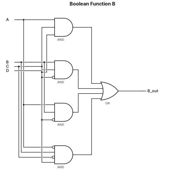
make a simple logic diagram for function B = ACD + BCD' + ABD' + A'BC'D. change what you already did.
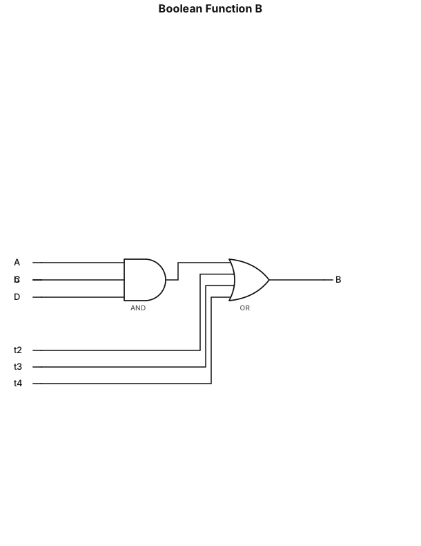
make a simple logic diagram for function B = ACD + BCD' + ABD' + A'BC'D. change what you already did. use small letter b instead of b_out
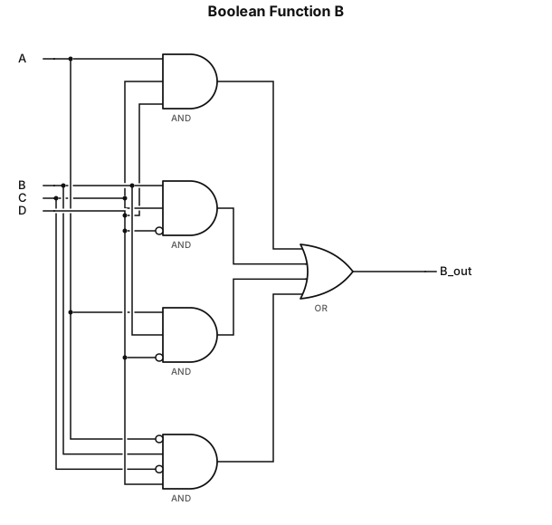
make a simple logic diagram for function B = ACD + BCD' + ABD' + A'BC'D. change what you already did
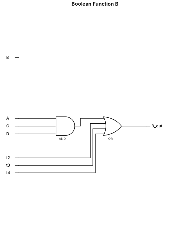
make a simple logic diagram for function B = ACD + BCD' + ABD' + A'BC'D
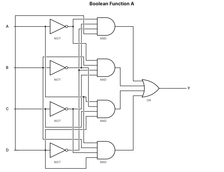
make a simple logic diagram for function A = A'B'C'D + A'BC'D' +AB'CD + ABC'D
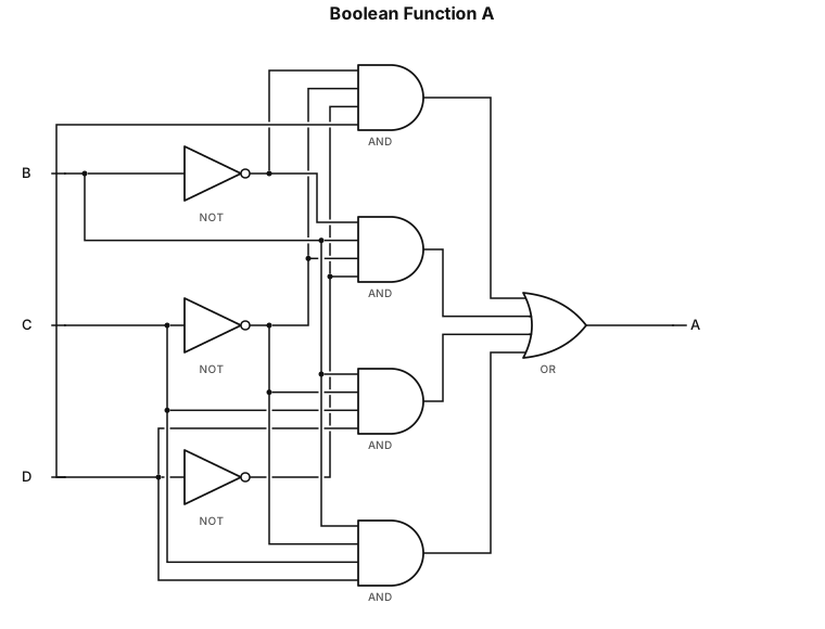
a logic diagram for a function A = A'B'C'D + A'BC'D' + AB'CD + ABC'D. use a instead of y in the output
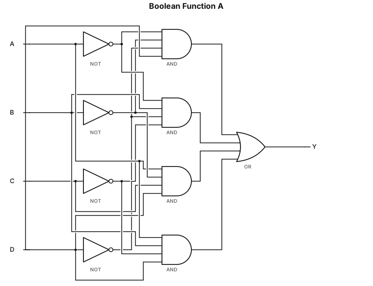
a logic diagram for a function A = A'B'C'D + A'BC'D' + AB'CD + ABC'D. make it like in proteus
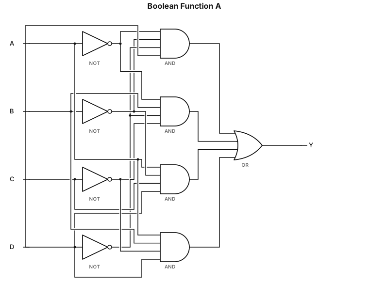
a logic diagram for a function A = A'B'C'D + A'BC'D' + AB'CD + ABC'D
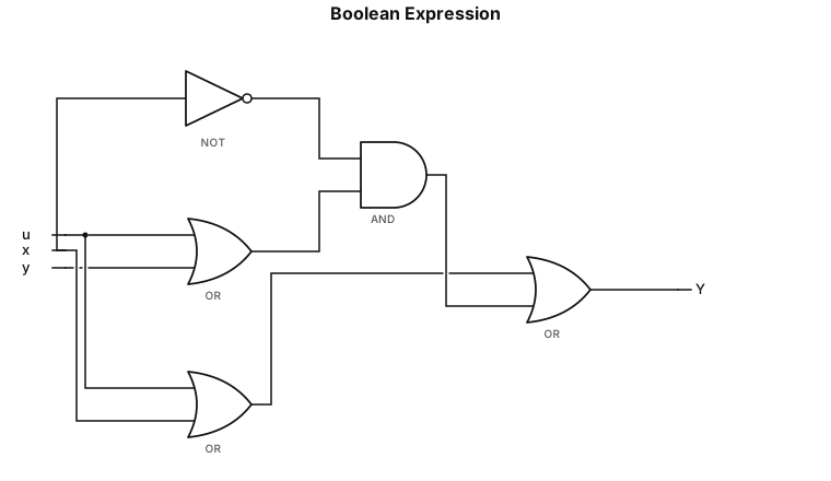
y= u+x+x'(u+y)
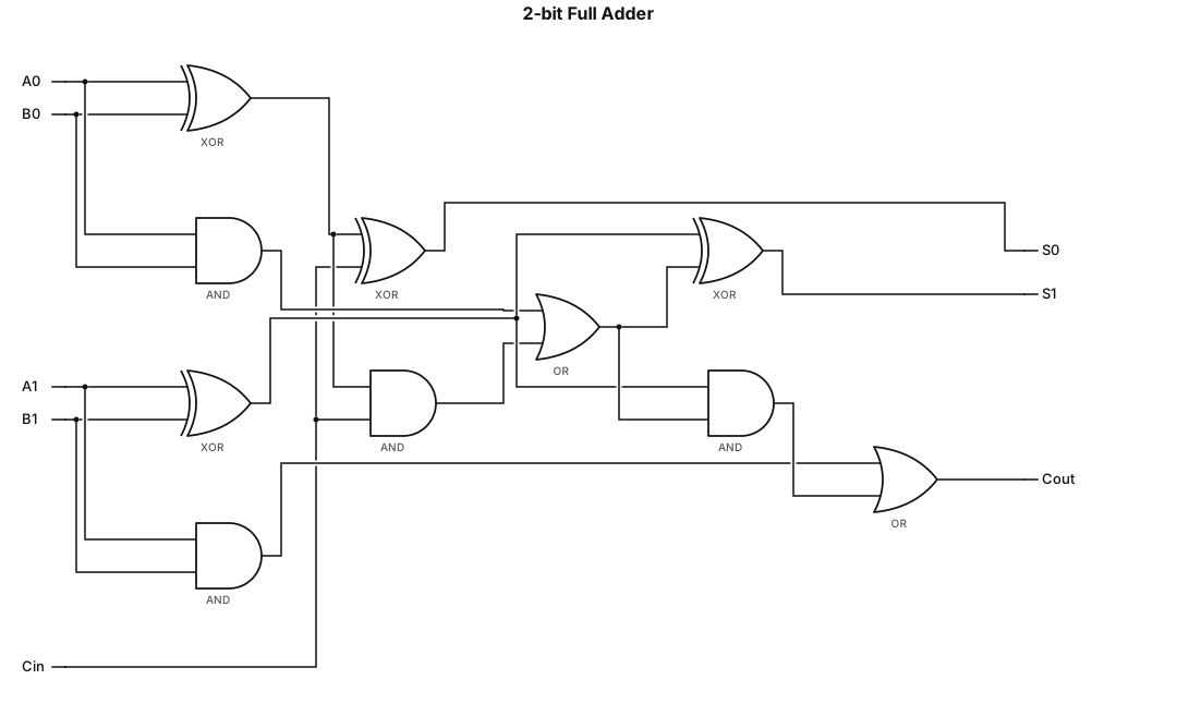
A logic gate circuit for a 2-bit full adder using AND, OR, and XOR gates with inputs A, B, and carry-in, and outputs sum and carry-outy= u+x+x'(u+y)
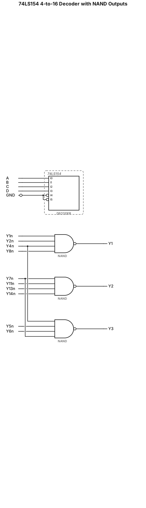
Digital logic diagram, chip 74LS154 4-to-16 decoder. Address input A3=A, A2=B, A1=C, A0=D. Enable pins SA' and SB' connect to GND. Decoder output Y1',Y2',Y4',Y8' connect to 4-input NAND gate, output Y1. Decoder output Y7',Y11',Y13',Y14' connect to second 4-input NAND gate, output Y2. Decoder output Y4',Y5',Y6',Y7' connect to third 4-input NAND gate, output Y3. Standard textbook circuit, black line, white background, neat wire.
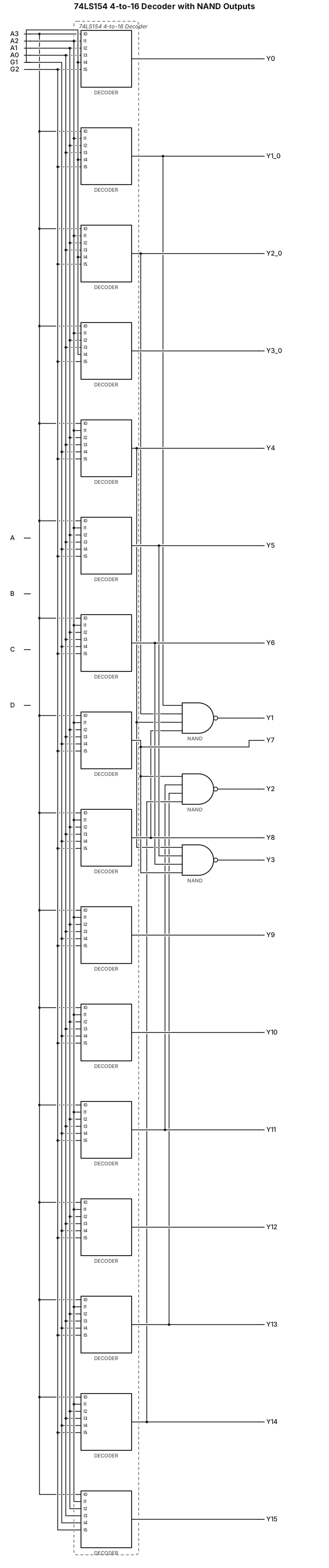
Draw digital logic circuit, include 74LS154 4-to-16 decoder chip. Input variables A,B,C,D connect to decoder address pins A3,A2,A1,A0. Chip enable pins G1 and G2 connect to ground(GND). Decoder output pins: Y1,Y2,Y4,Y8 connect to a 4-input NAND gate, gate output Y1. Y7,Y11,Y13,Y14 connect to second 4-input NAND gate, output Y2. Y4,Y5,Y6,Y7 connect to third 4-input NAND gate, output Y3. Standard IEEE circuit symbol, black lines on white background, neat straight wires, textbook style.
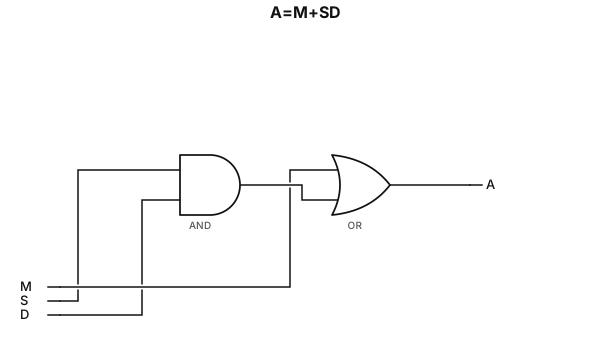
A=M+SD
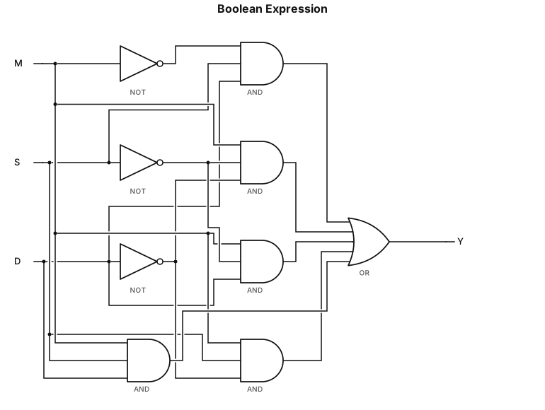
¯M SD+M¯S ¯D+M¯S D+MS¯D+MSD
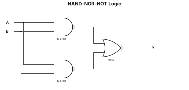
(A NAND B )(A NAND B) NOR NOT
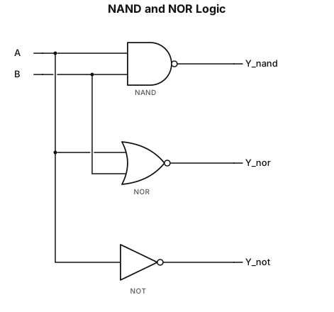
A NAND B A NAND B NOR NOT
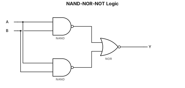
(A NAND B ) (A NAND B) NOR NOT
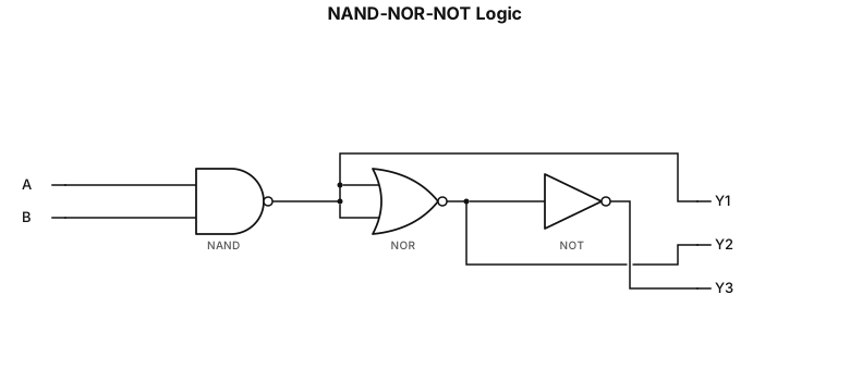
(A NAND B ) NOR(A NAND B) NOT
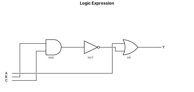
a or(b and c)not
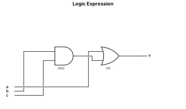
a+(b.c)^\
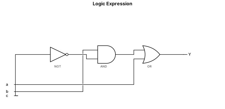
(b.c^\)+a
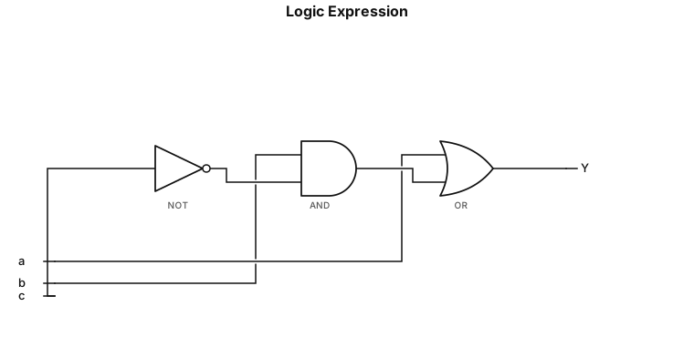
a+(b.c^\)
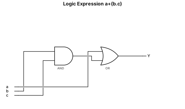
a+(b.c)\