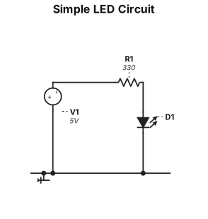
i want to make a simple circuit diagram
NODE ARCHIVE · REAL DIAGRAM BRIEFS
Diagram Examples from Real Visitor Prompts
Browse eligible diagrams shared by FreeDiagram visitors, inspect the exact prompts, and build your own version.
Browse 3261 real creationsCOMMUNITY OUTPUTS · EXACT PROMPTS
Circuit Diagrams
Showing 145–168 of 270. No stock examples or system defaults. Choose a tool, study a real result, then reopen its prompt as your starting point.
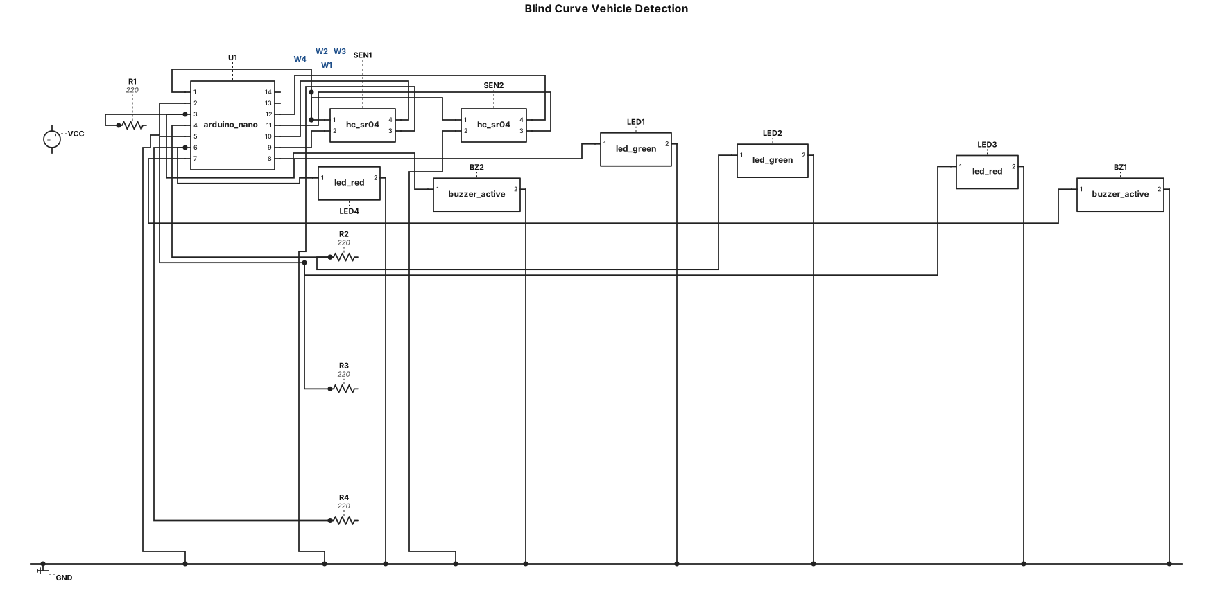
The circuit consists of two HC-SR04 ultrasonic sensors, an Arduino Nano, four LEDs, and two active buzzers. The ultrasonic sensors detect vehicles approaching the blind curve and send distance information to the Arduino Nano. The Arduino processes these inputs and determines whether a vehicle is present on either side. The green LEDs indicate a clear road, while the red LEDs and buzzers provide warnings when a vehicle is detected. If vehicles are detected on both sides simultaneously, both red LEDs and buzzers are activated to indicate a possible collision risk. Input → Processing → Output: HC-SR04 sensors → Arduino Nano → LEDs + Buzzers.
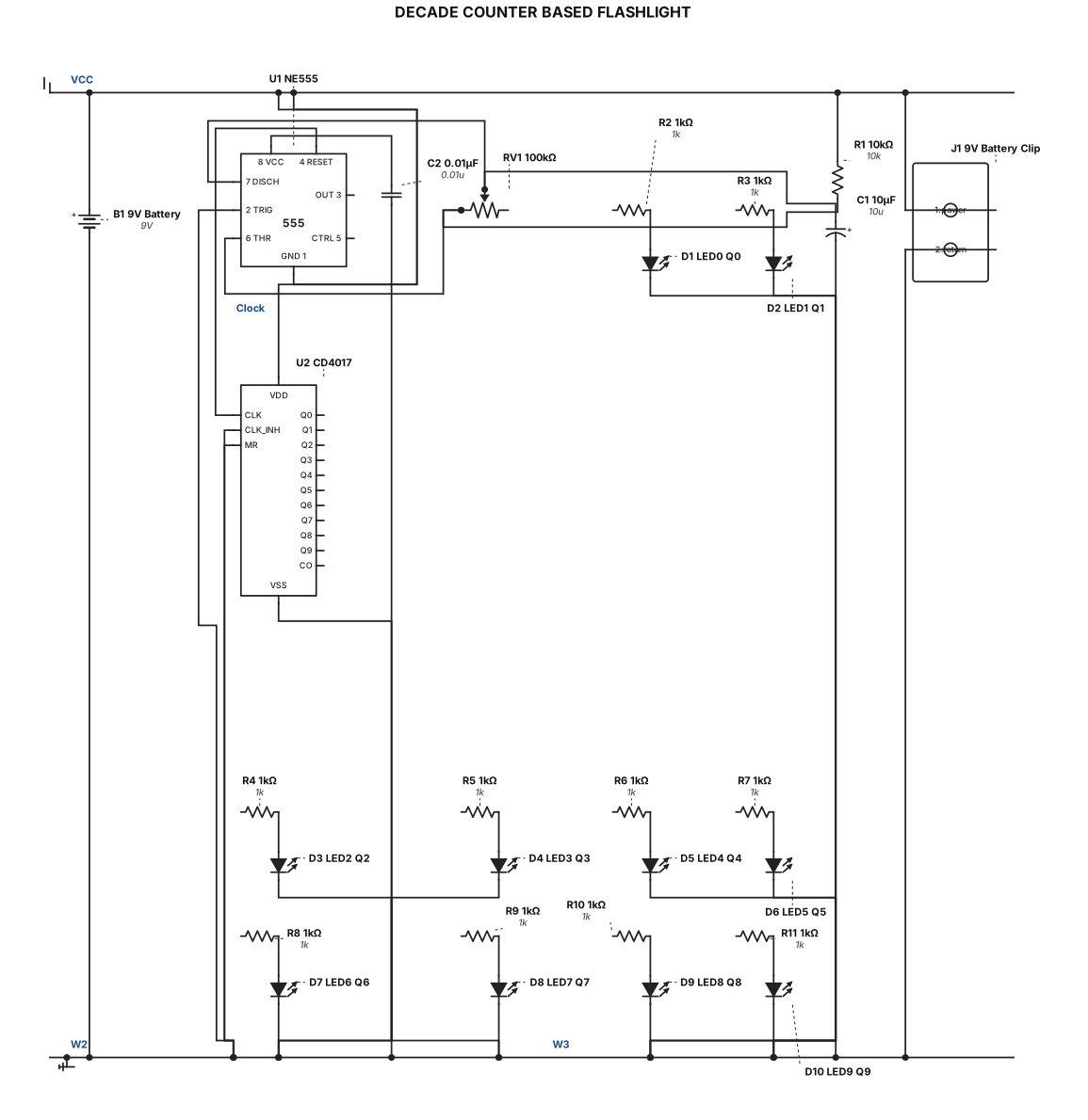
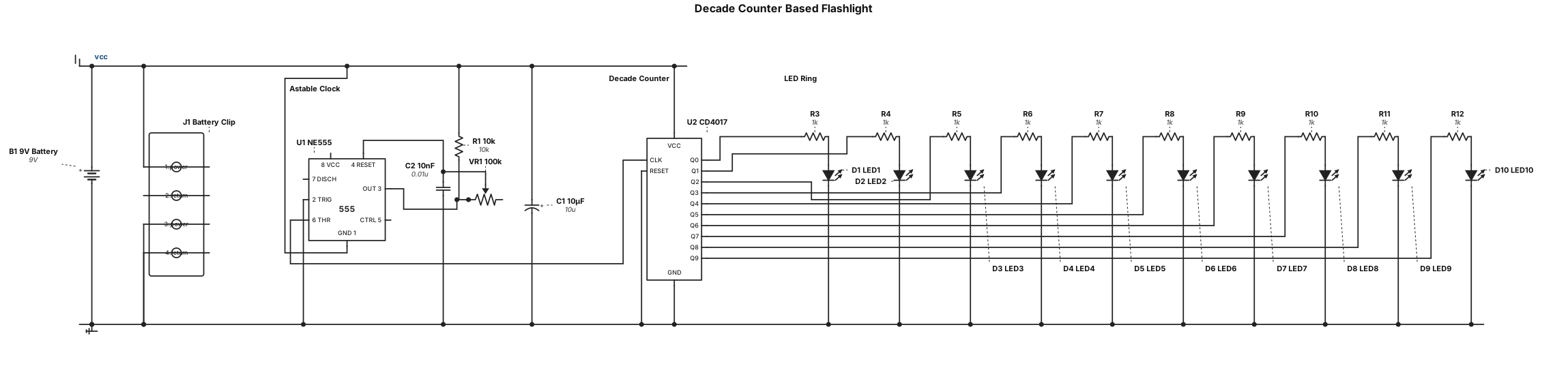
Create a technically accurate, clean electronic schematic titled “DECADE COUNTER BASED FLASHLIGHT”. Use ONLY these components: NE555 timer IC ×1, CD4017 decade counter IC ×1, 10 kΩ resistor ×1, 100 kΩ potentiometer ×1, 1 kΩ resistors ×10, 10 µF 16 V electrolytic capacitor ×1, 0.01 µF (10 nF) capacitor ×1, 5 mm LEDs ×10, 9 V DC battery ×1, 9 V battery clip ×1, solderless breadboard representation ×1, and jumper wires. Show the NE555 in astable mode producing a clock signal. Connect the 555 output to the CD4017 clock input. Show CD4017 outputs Q0, Q1, Q2, Q3, Q4, Q5, Q6, Q7, Q8 and Q9 individually connected to ten LEDs through ten separate 1 kΩ current-limiting resistors. Clearly show VCC and GND connections. Show the 100 kΩ potentiometer and 10 kΩ resistor in the 555 timing network, C1 10 µF as the timing capacitor and C2 0.01 µF as the control-pin capacitor. Clearly label every component, pin connection, Q0–Q9 output, clock connection, VCC, GND, battery positive and negative terminals. Use standard electronic schematic symbols, straight wires, no unnecessary components, white background, professional engineering drawing style.
Create a realistic college electronics project prototype titled “DECADE COUNTER BASED FLASHLIGHT”. Use ONLY these components: 1× NE555 timer IC, 1× CD4017 decade counter IC, 1× 10 kΩ resistor, 1× 100 kΩ potentiometer (VR1), 10× 1 kΩ resistors, 1× 10 µF 16 V electrolytic capacitor (C1), 1× 0.01 µF (10 nF) capacitor (C2), 10× 5 mm LEDs, 1× 9 V DC battery, 1× 9 V battery clip, 1× standard solderless breadboard, and male-to-male jumper wires. Do not add Arduino, ESP32, transistors, relays, switches, sensors, voltage regulators, extra ICs, or any other components. Show the NE555 configured as an astable oscillator generating clock pulses for the CD4017. Connect the CD4017 decade counter outputs Q0–Q9 to the ten LEDs, with one 1 kΩ resistor for each LED. Arrange the ten LEDs in an attractive circular flashlight pattern. Show the 9 V battery connected through the battery clip to the breadboard power rails. Make the prototype physically realistic, neatly wired, educational, suitable for an ECE college project exhibition, clear front three-quarter view, all components clearly visible and labeled, clean laboratory background, realistic breadboard wiring, no fictional components.
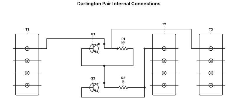
Draw the internal connections of Darlington pair.
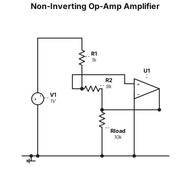
A non-inverting op-amp amplifier circuit with a gain of 10, using a 1 kΩ input resistor and a 9 kΩ feedback resistor
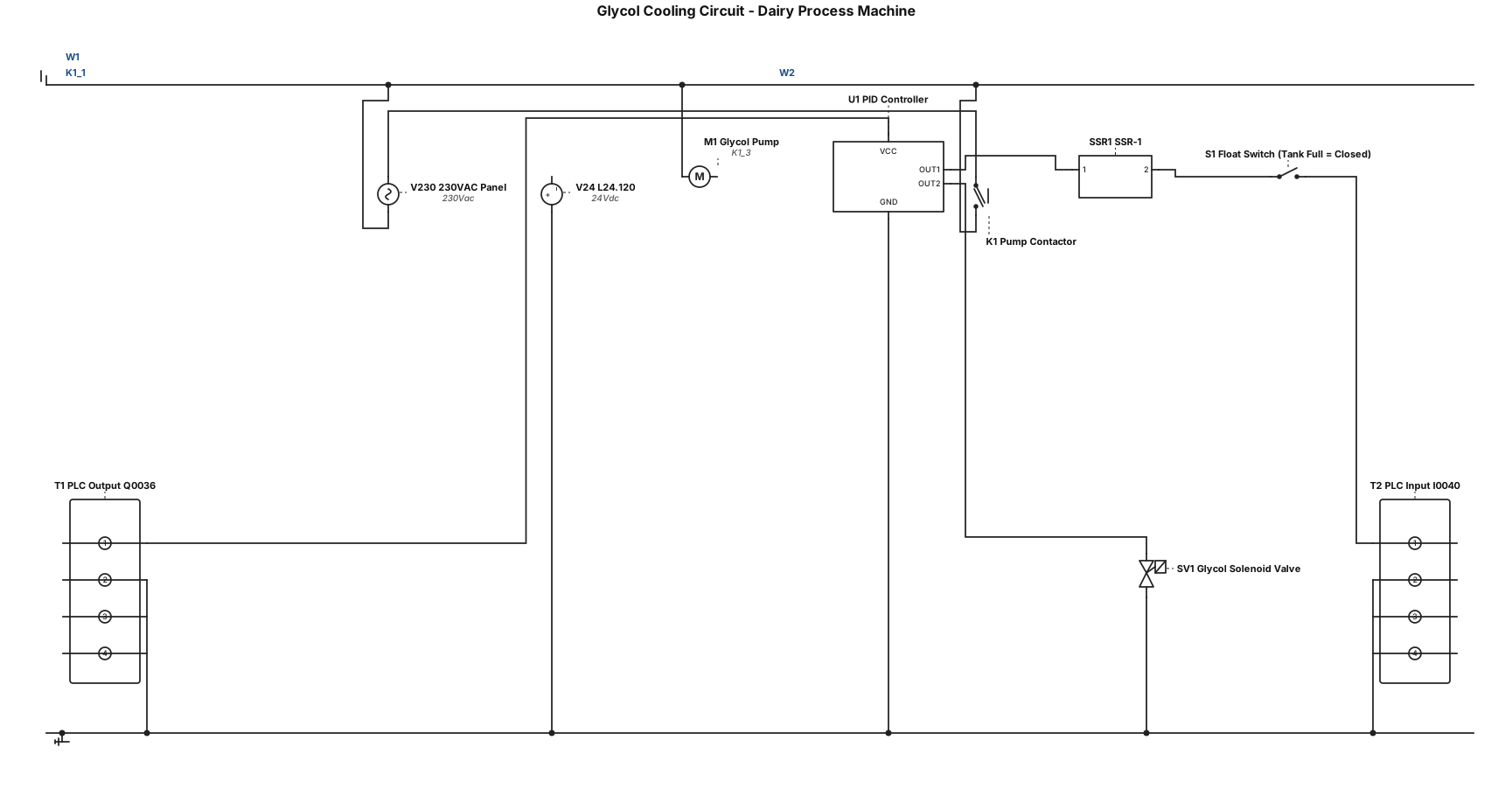
Glycol cooling circuit for dairy process machine. 24vdc from machine control panel (L24.120), To PID controller, out the PID controller, then through a solid state relay (SSR-1), Then into float switch (when tank full, switch is closed), this then feeds back to PLC input (I0040 - Alarm cooling circuit). also, 24V (L24.120) supplies another output on the pid controller, that output then goes to a glycol solenoid valve. There is also a pump, which is run through a 3 pole contactor, from 230vac (from the control panel). the solid state relay (SSR-1) coil is energised by the 230v from the pump contactor. also the PID controller power supply is ran from PLC output Q0036 (24vdc). NOTE: can you make the 24vdc line (L24.120), the i0040 PLC input line, and the Q0036 PLC ouput line all seperate on the drawing.
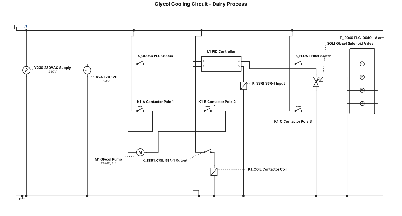
Glycol cooling circuit for dairy process machine. 24vdc from machine control panel (L24.120), To PID controller, out the PID controller, then through a solid state relay (SSR-1), Then into float switch (when tank full, switch is closed), this then feeds back to PLC input (I0040 - Alarm cooling circuit). also, 24V (L24.120) supplies another output on the pid controller, that output then goes to a glycol solenoid valve. There is also a pump, which is run through a 3 pole contactor, from 230vac (from the control panel). the solid state relay (SSR-1) coil is energised by the 230v from the pump contactor. also the PID controller power supply is ran from PLC output Q0036 (24vdc).
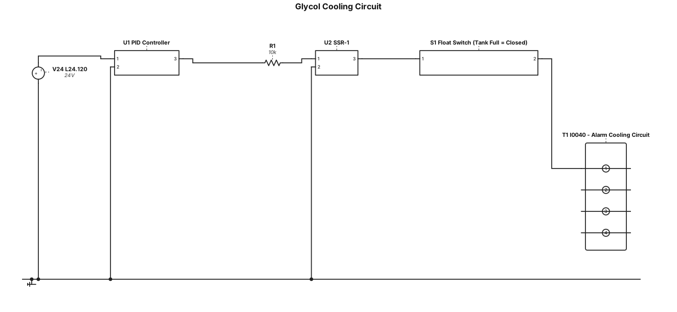
Glycol cooling circuit for dairy process machine. 24vdc from machine control panel (L24.120), To PID controller, out the PID controller, then through a solid state relay (SSR-1), Then into float switch (when tank full, switch is closed), this then feeds back to PLC input (I0040 - Alarm cooling circuit).
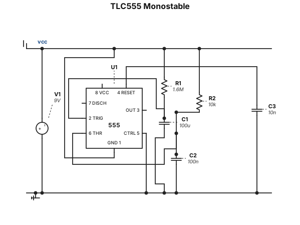
Fix this TLC555 monostable circuit. Pin 6 and Pin 7 MUST be directly connected together at ONE timing node. +9V → 1.6MΩ → timing node → 100µF → GND. Pin 2 MUST NOT connect to Pin 3 or the timing node. Pin 2 → 10kΩ → +9V. Pin 2 → 100nF → GND. Pin 3 is ONLY the output. Pin 5 → 10nF → GND. Pin 4 and Pin 8 → +9V. Pin 1 → GND. Show all connections clearly.
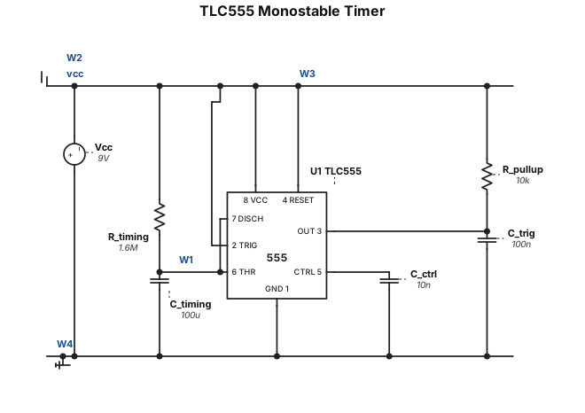
Create a correct TLC555 monostable timer. Pin 1→GND, Pin 8→+9V, Pin 4→+9V. Pin 5→10nF→GND. Pins 6 and 7 connected together. +9V→1.6MΩ→pins 6+7. Pins 6+7→100µF→GND. Pin 2→10kΩ→+9V and Pin 2→100nF→GND. Pin 3 is the timer output. Do not connect pins 6 or 7 directly to +9V. Show all pin numbers and values.
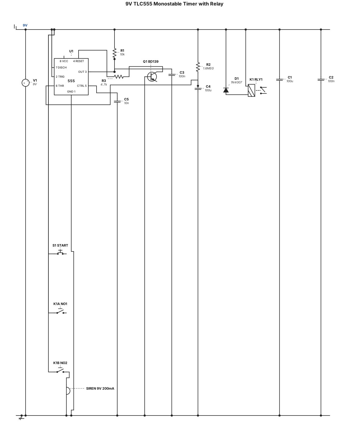
Create a correct buildable 9V TLC555 monostable timer, about 3 minutes. TLC555: pin 1 GND, pin 8 +9V, pin 4 +9V, pin 5 → 10nF → GND. Pins 6 and 7 together → timing node. +9V → 1.6MΩ → timing node → 100µF → GND. Pin 2 → 10kΩ → +9V and 100nF → GND for trigger. Pin 3 → 4.7kΩ → BD139 base. BD139 emitter → GND, collector → relay coil negative. 9V relay coil positive → +9V. 1N4007 directly across relay coil, cathode → +9V. Use 2 NO relay contacts: NO1 connects battery +9V to switched +9V for self-holding, parallel to START. NO2 switches a 9V 200mA siren. Siren negative → GND. After ~3 minutes the relay turns off and disconnects the timer. Show exact pin numbers and all connections. Do not change these connections.
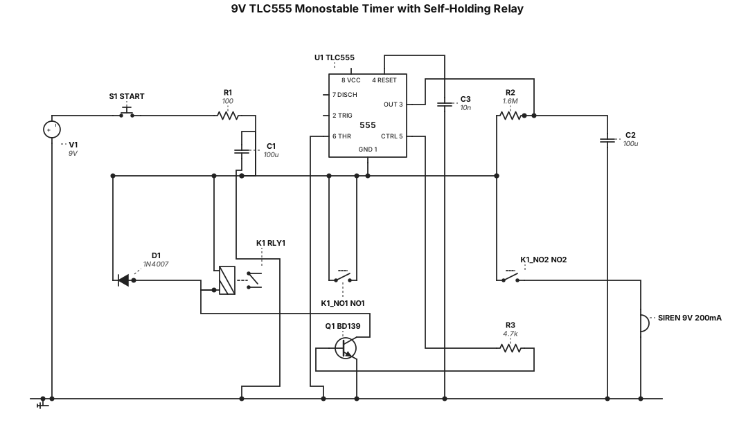
Create a correct, buildable 9V TLC555 monostable timer. Pin 1→GND, 8→+9V, 4→+9V, 5→10nF→GND. Pins 6+7→timing node. +9V→1.6MΩ→timing node→100µF→GND. Pin 2 gets a short LOW trigger from the START button. Pin 3→4.7kΩ→BD139 base. BD139 emitter→GND, collector→negative relay coil. 9V relay coil positive→+9V. 1N4007 directly across coil: cathode→+9V, anode→collector. Relay has 2 NO contacts: NO1 self-holds the timer power in parallel with START. NO2 switches a 9V 200mA siren. After ~3 minutes the relay turns off and disconnects the timer. Show exact TLC555 pin numbers and all connections. Do not change the topology.
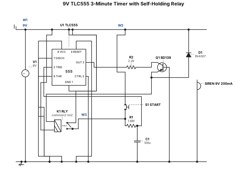
Create a simple 9V timer circuit with a TLC555. Press a push button to start a 3-minute timer. Use 1.6MΩ and 100µF for timing. TLC555 output drives a BD139 transistor through 2.2kΩ. BD139 drives a 9V relay coil. Add a 1N4007 flyback diode across the relay coil. Use a relay with two normally-open contacts: 1. Contact 1 self-holds the circuit after the button is released. 2. Contact 2 switches a 9V 200mA siren. After 3 minutes the relay turns off, the siren stops, and the timer loses power. Show all TLC555 pin numbers, component values, +9V and GND.
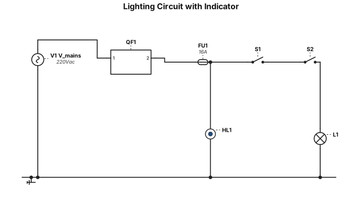
Create a simple electrical lighting circuit schematic with exactly 6 components: QF1 — circuit breaker FU1 — fuse S1 — switch S2 — switch L1 — light bulb HL1 — indicator lamp Use standard electrical schematic symbols. Connect the circuit so that QF1 and FU1 are in series with the switches. S1 and S2 control the light bulb, and HL1 is connected as an indicator. Show clear wires and component labels. Use a clean 2D schematic layout.
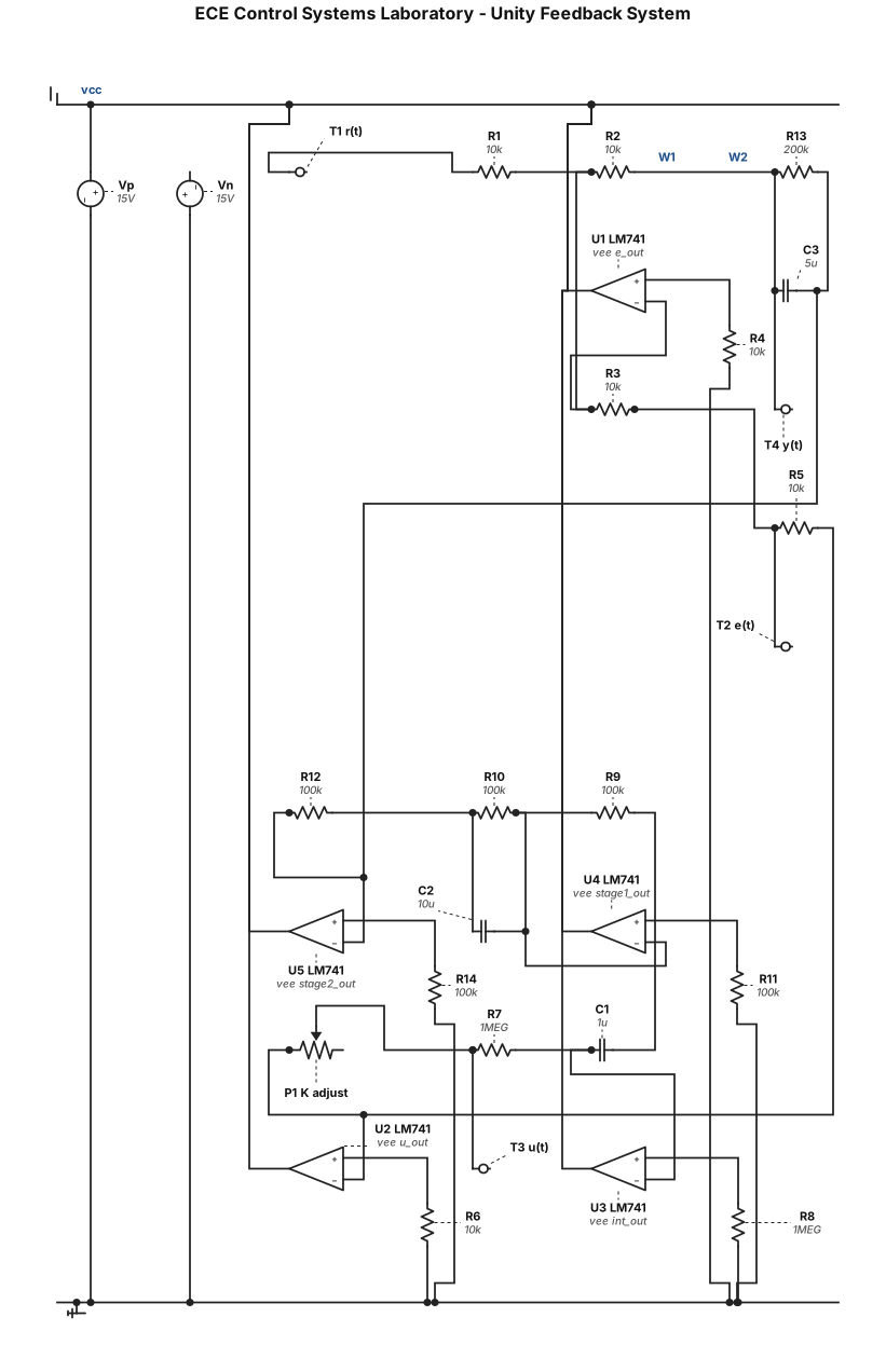
Draw a clean, professional electrical schematic for an ECE control-systems laboratory. Use five LM741 op-amps powered by +15 V and -15 V. The circuit must implement a unity negative-feedback system with: Plant: Gp(s) = 1 / [s(s+1)(s+2)] Controller: u(t) = K[r(t) - y(t)] Circuit sections from left to right: 1. A differential amplifier using matched 10 kΩ resistors that produces: e(t) = r(t) - y(t) 2. A proportional op-amp controller with a potentiometer to adjust K from 0 to 7: u(t) = K e(t) 3. An op-amp integrator with Rin = 1 MΩ and C = 1 μF: transfer function 1/s 4. An active first-order RC stage: transfer function 1/(s+1) 5. An active first-order RC stage: transfer function 1/(s+2) Connect the plant output y(t) back to the negative input of the differential amplifier. Show all LM741 pins, resistor values, capacitor values, potentiometer, +15 V supply, -15 V supply, and ground connections. Label all test points: r(t), e(t), u(t), and y(t). Use standard schematic symbols, straight orthogonal wires, no unnecessary crossings, and a clean left-to-right layout. Make sure the overall plant polarity is positive.
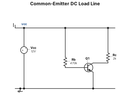
A clean educational graph on a white background showing the DC load line of a common-emitter transistor amplifier. The vertical axis is labeled "Ic (mA)" and the horizontal axis is labeled "Uce (V)". A straight diagonal line goes from the Y-axis to the X-axis. A clear dot on the middle of this line is marked as "Q-point". Minimalist, technical engineering style, monochromatic black and white.
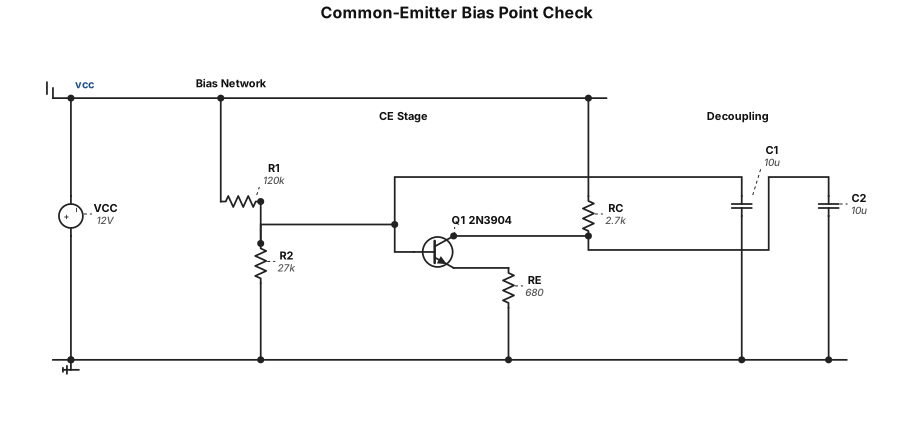
Схема для проверки рабочей точки транзисторного каскада с ОЭ в симуляторе: NPN 2N3904, питание 12 V, R1 = 120 kΩ, R2 = 27 kΩ, Rк = 2.7 kΩ, Rэ = 680 Ω; рядом компактно показать три мини-таблицы или три подписи для β = 100, 200 и 300 с токами Iк и напряжениями Uкэ; выделить рабочую точку Q на нагрузочной прямой; белый фон, аккуратный инженерный стиль, без лишнего текста.
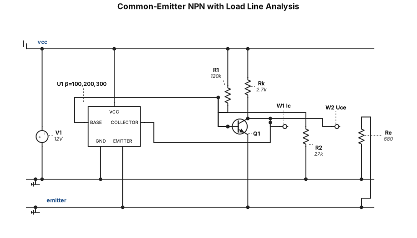
A technical engineering diagram on a white background with a faint light blue grid, combining a common-emitter NPN transistor circuit with an analytical chart and graph. The left side shows the circuit: a 12V DC source, base voltage divider with resistors R1=120kΩ and R2=27kΩ, an NPN transistor, collector resistor Rk=2.7kΩ, and emitter resistor Re=680Ω. To the right of the circuit, there is a small, neat data table listing three rows for beta (β) values: 100, 200, and 300, with columns for Ic and Uce. Below the table, a small conceptual load line graph (Vce vs Ic) highlights the operating Q-point. Clean vector style, monochromatic black lines for the circuit, professional educational layout, standard IEEE/IEC symbols.
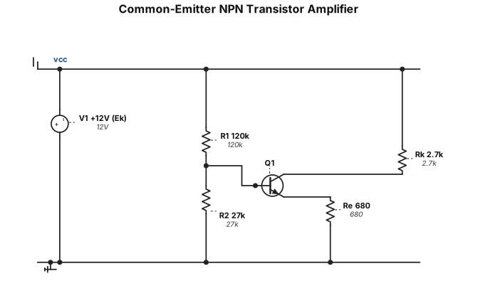
A clean, technical electronic circuit schematic of a common-emitter NPN transistor amplifier on a white background with a faint light blue grid. A top horizontal wire represents the power rail, connected to a DC source labeled 'V1 +12V (Ek)'. A bottom horizontal wire is connected to a ground symbol. A voltage divider consisting of two zigzag resistors, 'R1 120k' (top) and 'R2 27k' (bottom), is connected to the base of an NPN transistor labeled 'Q1'. A zigzag collector resistor 'Rk 2.7k' connects the top rail to the transistor's collector. A zigzag emitter resistor 'Re 680' connects the transistor's emitter to the bottom ground rail. Minimalist, professional engineering style, monochromatic black lines, standard IEEE/IEC symbols, neat layout.
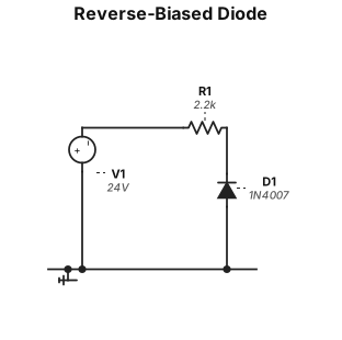
**Английский промт для генерации схемы обратного включения диода:** > *A clean, technical electronic circuit schematic based on image_3.png, presented on a white background with a subtle grid. A vertical DC voltage source is shown on the left, labeled 'V1 24V', with its negative terminal at the bottom connected to a solid ground line with a standard IEEE/IEC ground symbol. From the positive terminal of V1, a neat right-angle wire connects to a horizontal, zig-zag resistor symbol labeled 'R1 2.2 kΩ'. Following the resistor, a vertical wire extends downwards, connecting to a diode. Crucially, this diode (labeled 'D1 1N4007') is oriented with its cathode (the line-side of the triangle symbol) facing upwards, towards the source, representing reverse bias. The anode of D1 connects to the same ground line. All labels use clean, monochromatic technical typography.*
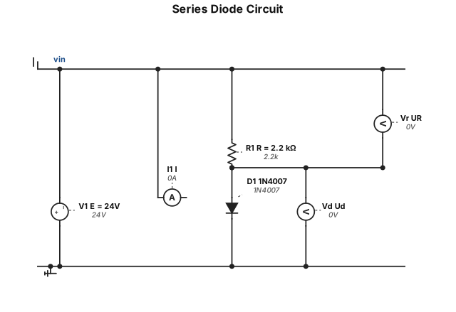
A clean, professional black and white electronic circuit schematic on a white background. Educational laboratory style. A DC voltage source labeled "E = 24V", connected in series to a resistor "R = 2.2 kΩ", and a silicon diode "1N4007" pointing right, ending in a ground symbol. Include a current arrow labeled "I" and voltage labels "Ud" and "UR". Standard IEEE/IEC symbols, minimalist, neat horizontal layout.
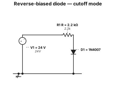
Create a clean educational electrical schematic on a white background using standard diode symbols. Show one simple series circuit: a 24 V DC voltage source, a 2.2 kΩ resistor, and a 1N4007 diode connected in series to ground. The diode must be reverse-biased. Rotate the diode 180 degrees compared with a forward-biased circuit: the cathode bar MUST be at the top, directly connected to the resistor and the positive side of the 24 V source; the anode MUST be at the bottom, connected toward ground. The cathode bar must be clearly visible above the diode symbol. Do not place the cathode bar near ground. Do not add any extra current source, parallel branch, measuring instrument, or additional wires. Show only one closed series loop. Label the components exactly: “V1 = 24 V” “R = 2.2 kΩ” “D1 = 1N4007” Add the text “Reverse-biased diode — cutoff mode”. Remove all unwanted labels, placeholder text, duplicate values, and text such as “Wlabel”. Use a neat technical style with black circuit lines, clear labels, and a white background.
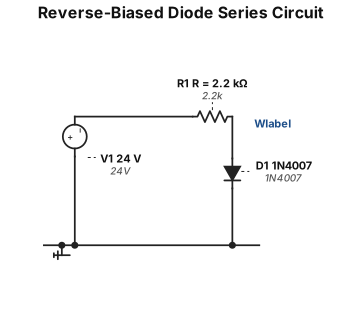

Create a clean educational electrical schematic on a white background using standard IEC circuit symbols. Show one simple series circuit only: a 24 V DC voltage source, a 2.2 kΩ resistor, and a 1N4007 diode connected in series to ground. The diode must be reverse-biased: connect the cathode, marked by the diode bar, toward the resistor and the positive terminal of the 24 V source; connect the anode toward ground. Do not add any extra current source, parallel branch, measuring instrument, or additional wires. Show only one closed series loop. Label the source “24 V”, the resistor “R = 2.2 kΩ”, and the diode “D1 1N4007”. Add a small label near the diode: “Reverse current ≈ 0, cutoff mode”. Use a neat horizontal layout, black circuit lines, clear technical labels, and no decorative elements.