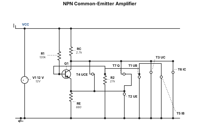
Create a clean educational circuit schematic on a white background using standard IEC symbols. Show an NPN transistor, such as a 2N3904 or BC547, in a common-emitter amplifier configuration. Use a 12 V DC power supply. Connect R1 = 120 kΩ from the positive supply to the transistor base and R2 = 27 kΩ from the base to ground. Connect the collector through R_C = 2.7 kΩ to the positive supply. Connect the emitter through R_E = 680 Ω to ground. Label the base, emitter, and collector voltages as U_B, U_E, and U_C. Also label U_CE, base current I_B, collector current I_C, and the operating point Q. Use straight wires, clear labels, black circuit lines, and no decorative background.
NODE ARCHIVE · REAL DIAGRAM BRIEFS
Diagram Examples from Real Visitor Prompts
Browse eligible diagrams shared by FreeDiagram visitors, inspect the exact prompts, and build your own version.
Browse 3262 real creationsCOMMUNITY OUTPUTS · EXACT PROMPTS
Circuit Diagrams
Showing 169–192 of 270. No stock examples or system defaults. Choose a tool, study a real result, then reopen its prompt as your starting point.
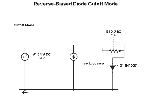
Create a clean educational electrical schematic on a white background using standard IEC circuit symbols. Show a 24 V DC voltage source, a 2.2 kΩ resistor, and a 1N4007 diode connected in series to ground, but reverse the diode polarity. Clearly show the cathode toward the voltage source and the anode toward ground. Mark the very small reverse current I_reverse and label the circuit state as “cutoff mode”. Use a black-and-white technical style with clear component labels and no decorative elements.
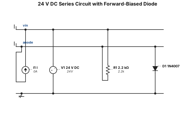
Create a clean educational electrical schematic on a white background using standard IEC circuit symbols. Show a 24 V DC voltage source connected in series to a 2.2 kΩ resistor, then to a silicon 1N4007 diode, and finally to ground. The diode must be forward-biased, with the anode connected toward the resistor and the cathode connected toward ground. Mark the current direction with an arrow and label the voltage across the diode as U_D and the voltage across the resistor as U_R. Use a neat horizontal layout, black circuit lines, clear technical labels, and no decorative elements.
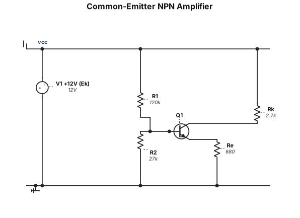
A clean, professional electronic circuit schematic of a common-emitter NPN transistor amplifier. Top rail is labeled "+12V (Ek)". A voltage divider with resistors R1 (120k) and R2 (27k) is connected to the base of the NPN transistor. Collector resistor Rk (2.7k) connects the collector to the +12V rail. Emitter resistor Re (680 Ω) connects the emitter to ground. Standard IEEE electrical symbols, monochromatic, technical drawing style, white background.
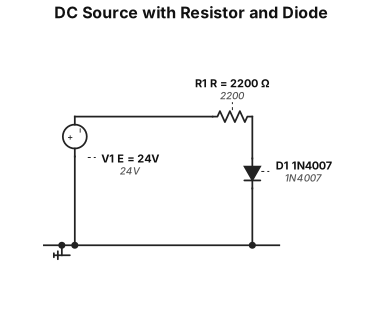
A clean, professional black and white electronic circuit schematic on a white background. The circuit consists of a single loop. On the left, a DC voltage source labeled "E = 24V". Connected in series clockwise: a resistor on the top labeled "R = 2200 Ω", a standard semiconductor diode on the right side pointing downwards labeled "1N4007", and a ground symbol at the bottom negative return path. Standard IEEE/IEC electrical symbols, minimalist, high contrast.
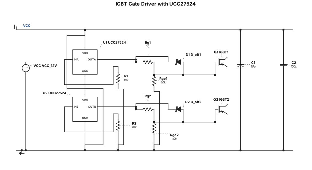
i have to make one circuit using UCC27524 for my IGBT driving applications, suggest circuit
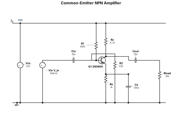
A common-emitter NPN transistor amplifier circuit
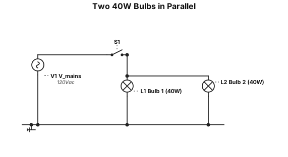
two 40 watt light bulbs connected in parallel in light fixture, powered by 120v of electricity for 150 hours at $0.12 per Kw-hr
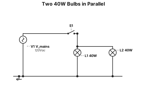
two 40 watt light bulbs connected in parallel in light fixture, powered by 120v of electricity
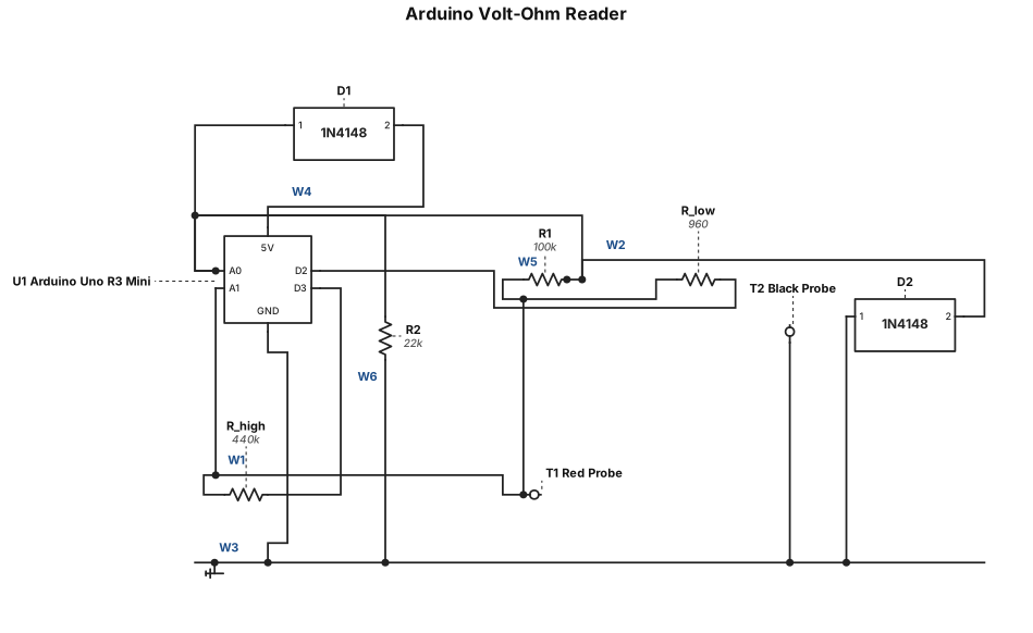
a volt and ohm reader for arduino uno r3 mini that has 2x100k resistors, 1x22k resistor, 1x1k resistor and 2x1N4148 diodes, like this: Step 0: Prepare and label your Arduino-side wires first Cut 6 short wires, solder one end of each into its confirmed hole (per the continuity check from before), and label the free end with a bit of tape so you never lose track: Wire "A0" Wire "A1" Wire "D2" Wire "D3" Wire "5V" Wire "GND" Do this one at a time, and re-check continuity from the Arduino header pin to the wire's free end after each solder joint — confirms you didn't just cold-solder it. Step 1: Build "Node P" — the probe/A1 junction (5 leads meet here) Twist these 5 things together tightly, then solder as one joint: Wire "A1" Red probe wire One leg of R1 (100k) One leg of R_low (your 960Ω) One leg of R_high (your twisted 220k+220k pair — treat both legs on this end as already joined into one lead) Step 2: Build "Node V" — the voltage divider midpoint (5 leads meet here) Twist and solder together: Wire "A0" R1's other leg (opposite end from Node P) One leg of R2 (22k) Diode 1's anode (the end without the stripe) Diode 2's cathode (the end with the stripe) ⚠️ Double-check diode orientation here specifically — this is the step most likely to cause a problem if flipped. Step 3: Build the "GND" node (4 leads meet here) Twist and solder together: Wire "GND" Black probe wire R2's other leg Diode 2's anode (no stripe) Step 4: Build the "5V" node (2 leads — simplest joint) Twist and solder together: Wire "5V" Diode 1's cathode (striped end) Step 5: Two simple 2-lead joints (no hub, just direct pairs) Wire "D2" + R_low's other leg (opposite end from Node P) — solder directly together Wire "D3" + R_high's other leg — solder directly together
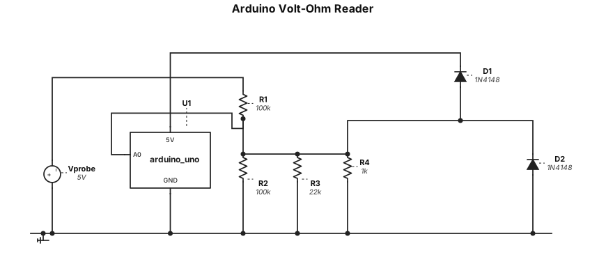
a volt and ohm reader for arduino uno r3 mini that has 2x100k resistors, 1x22k resistor, 1x1k resistor and 2x1N4148 diodes
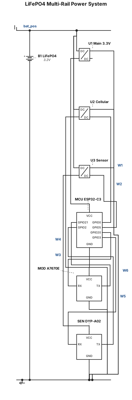
Component List: B1: LiFePO4 Battery 3.2v U1: Main 3.3V Boost Converter U2: Booster 1 (Cellular Power) U3: Booster 2 (Sensor Power) MCU: ESP32-C3 SuperMini MOD: A7670E Cellular Module SEN: DYP-A02 Sensor Power Wiring: B1 Positive -> U1 VIN B1 Positive -> U2 VIN B1 Positive -> U3 VIN U1 VOUT -> MCU VCC U2 VOUT -> MOD VCC U3 VOUT -> SEN VCC Ground Wiring (Common Ground): B1 Negative -> Common GND U1 GND -> Common GND U2 GND -> Common GND U3 GND -> Common GND MCU GND -> Common GND MOD GND -> Common GND SEN GND -> Common GND Control Logic (Enable Pins): MCU GPIO 0 -> U2 EN MCU GPIO 5 -> U3 EN UART Data Wiring: MCU GPIO 20 -> MOD RX MCU GPIO 21 -> MOD TX MCU GPIO 2 -> SEN TX MCU GPIO 3 -> SEN RX
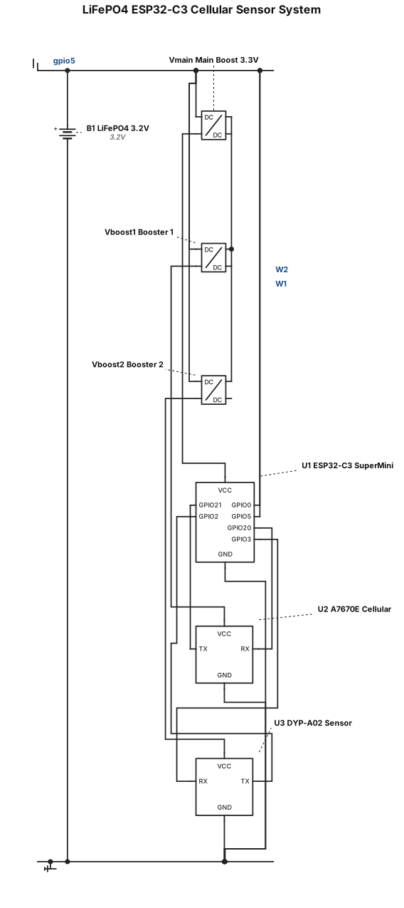
Hardware Components List 1x 3.2V LiFePO4 Battery 1x ESP32-C3 SuperMini 1x Main 3.3V Boost Converter (Always-on) 2x Switched Boost Converters (Booster 1 and Booster 2) 1x A7670E Cellular Module 1x DYP-A02 Sensor Wiring & Connections Power (VIN & GND) LiFePO4 Battery Positive (+) connects to the VIN of the Main 3.3V Boost Converter, Booster 1, and Booster 2. LiFePO4 Battery Negative (-) connects to a Common Ground bus. Common Ground connects to the GND pins of the ESP32-C3, all three Boost Converters, the A7670E, and the DYP-A02. Power Distribution (VOUT) Main 3.3V Boost Converter VOUT connects to ESP32-C3 VIN/VCC (Always-on power). Booster 1 VOUT connects to A7670E VCC (Duty-cycled power). Booster 2 VOUT connects to DYP-A02 VCC (Duty-cycled power). Control Pins (Enable Lines) ESP32-C3 GPIO 0 connects to Booster 1 EN (Enable). ESP32-C3 GPIO 5 connects to Booster 2 EN (Enable). Data Pins (UART Communication) ESP32-C3 GPIO 20 connects to A7670E RX. ESP32-C3 GPIO 21 connects to A7670E TX. ESP32-C3 GPIO 2 connects to DYP-A02 TX. ESP32-C3 GPIO 3 connects to DYP-A02 RX.
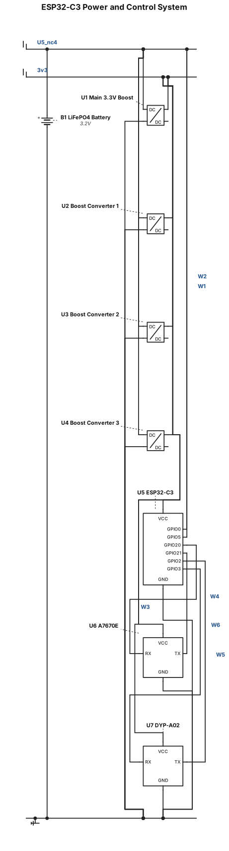
1. Power Connections LiFePO4 Battery (+ Terminal) Connects to VIN of the Main 3.3V Boost Converter. Connects in parallel to VIN of Boost Converter 1, Boost Converter 2, and Boost Converter 3. Ground (GND) Battery (-) connects to a Common Ground wire/bus. ESP32-C3 GND \rightarrow Common Ground. A7670E GND \rightarrow Common Ground. DYP-A02 GND \rightarrow Common Ground. All Boost Converter GND pins \rightarrow Common Ground. 2. Control Lines (Enable Pins) ESP32-C3 GPIO 0 \rightarrow EN (Enable) pin of Boost Converter 1 ESP32-C3 GPIO 5 \rightarrow EN (Enable) pin of Boost Converter 2 (Note: Booster 3 EN is unassigned here or wired permanently ON). 3. Data / Communication Lines (UART) A7670E Cellular Module: ESP32-C3 GPIO 20 \rightarrow A7670E RX pin ESP32-C3 GPIO 21 \rightarrow A7670E TX pin DYP-A02 Ultrasonic Sensor: ESP32-C3 GPIO 2 \rightarrow DYP-A02 TX pin ESP32-C3 GPIO 3 \rightarrow DYP-A02 RX pin
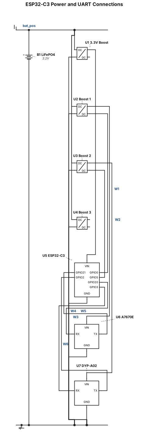
Power & Supply * LiFePO4 Battery 3.2v (+) > VIN of 3.3V Boost Converter & VIN of 1, 2 & 3 boost converters * Common Ground > Shared across all components (ESP32-C3, battery, boost converters, A7670E, DYP-A02) * Boost Converter Enable (EN) Pins * ESP32-C3 GPIO 0 > Booster 1 EN * ESP32-C3 GPIO 5 > Booster 2 EN * A7670E Cellular Module (UART) * ESP32-C3 GPIO 20 > A7670E RX * ESP32-C3 GPIO 21 > A7670E TX * DYP-A02 Sensor (UART) * ESP32-C3 GPIO 2 > DYP-A02 TX * ESP32-C3 GPIO 3 > DYP-A02 RX
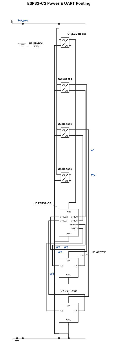
Power & Supply * LiFePO4 Battery 3.2v (+) to VIN of 3.3V Boost Converter & VIN of 3 boost converters * Common Ground to Shared across all components (ESP32-C3, battery, boost converters, A7670E, DYP-A02) * Boost Converter Enable (EN) Pins * ESP32-C3 GPIO 0 > Booster 1 EN * ESP32-C3 GPIO 5 > Booster 2 EN * A7670E Cellular Module (UART) * ESP32-C3 GPIO 20 > A7670E RX * ESP32-C3 GPIO 21 > A7670E TX * DYP-A02 Sensor (UART) * ESP32-C3 GPIO 2 > DYP-A02 TX * ESP32-C3 GPIO 3 > DYP-A02 RX
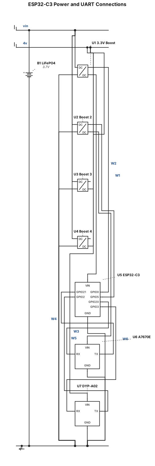
Power & Supply * LiFePO4 Battery (+) \rightarrow VIN of 3.3V Boost Converter & VIN of 3 boost converters * Common Ground \rightarrow Shared across all components (ESP32-C3, battery, boost converters, A7670E, DYP-A02) * Boost Converter Enable (EN) Pins * ESP32-C3 GPIO 0 \rightarrow Booster 1 EN * ESP32-C3 GPIO 5 \rightarrow Booster 2 EN * A7670E Cellular Module (UART) * ESP32-C3 GPIO 20 \rightarrow A7670E RX * ESP32-C3 GPIO 21 \rightarrow A7670E TX * DYP-A02 Sensor (UART) * ESP32-C3 GPIO 2 \rightarrow DYP-A02 TX * ESP32-C3 GPIO 3 \rightarrow DYP-A02 RX
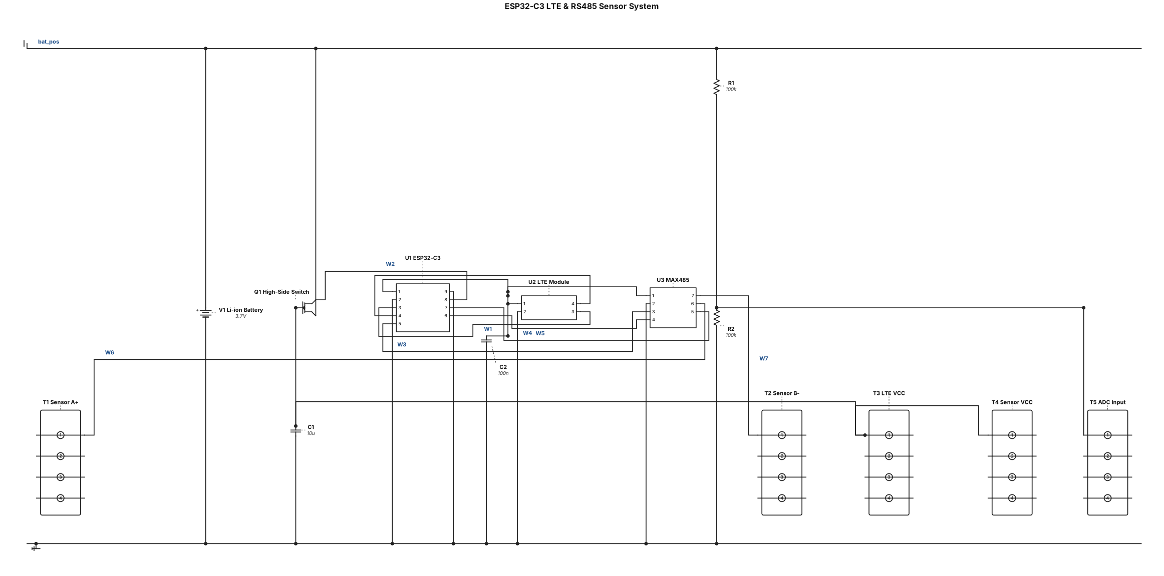
ESP32-C3 Pinout & Wiring Connections LTE Module (UART) ESP32 GPIO 21 (TX) \rightarrow LTE Module RX ESP32 GPIO 20 (RX) \rightarrow LTE Module TX Area-Velocity Sensor via RS485 Transceiver (MAX485) ESP32 GPIO 4 (TX) \rightarrow MAX485 DI (Driver Input) ESP32 GPIO 5 (RX) \rightarrow MAX485 RO (Receiver Output) ESP32 GPIO 6 \rightarrow MAX485 DE / RE (Data Enable / Receive Enable) MAX485 A \rightarrow Sensor RS485 A (+) MAX485 B \rightarrow Sensor RS485 B (-) Power Switching (MOSFET Control) ESP32 GPIO 3 \rightarrow MOSFET Gate (Controls high-side power switch for LTE & Sensor VCC) Battery Voltage Monitor (ADC) ESP32 GPIO 0 (ADC1_CH0) \rightarrow Resistor Voltage Divider midpoint (Connected to Battery V+) Power & Ground Rails ESP32 3V3 \rightarrow Regulated 3.3V DC Output (from DC-DC Buck Converter) ESP32 GND \rightarrow Common System Ground (Shared with Battery Negative, DC-DC GND, LTE GND, and Sensor GND)
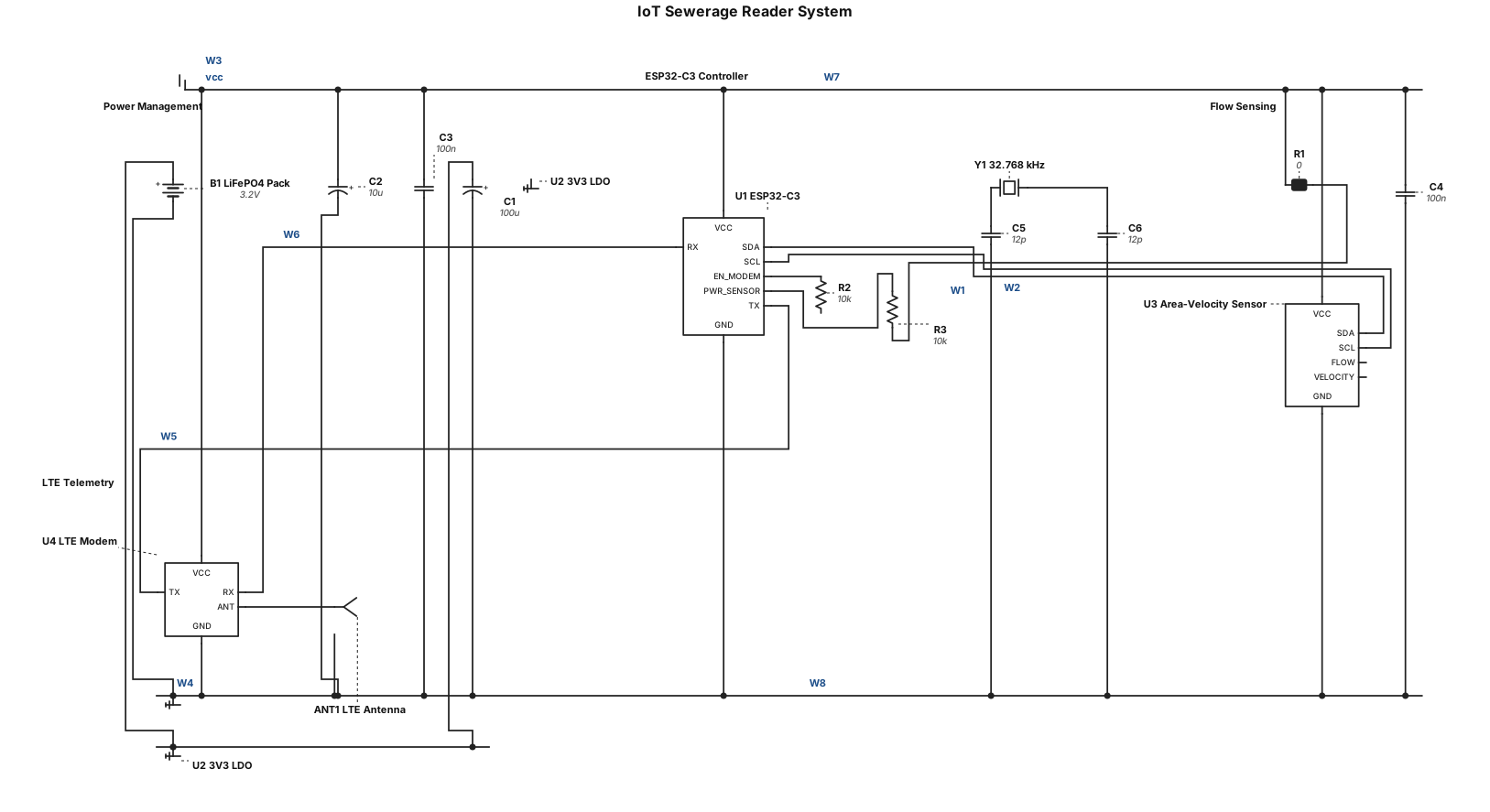
Generate a comprehensive technical system architecture and data-flow diagram for an IoT sewerage reader device. The system features an ESP32-C3 microcontroller powered by a LiFePO4 battery pack, connected to an area-velocity flow sensor and an LTE telemetry module. Include a duty-cycle state machine that wakes from deep sleep, polls sensors, evaluates blockage/flow thresholds, powers up the cellular modem to transmit data, and returns to deep sleep.
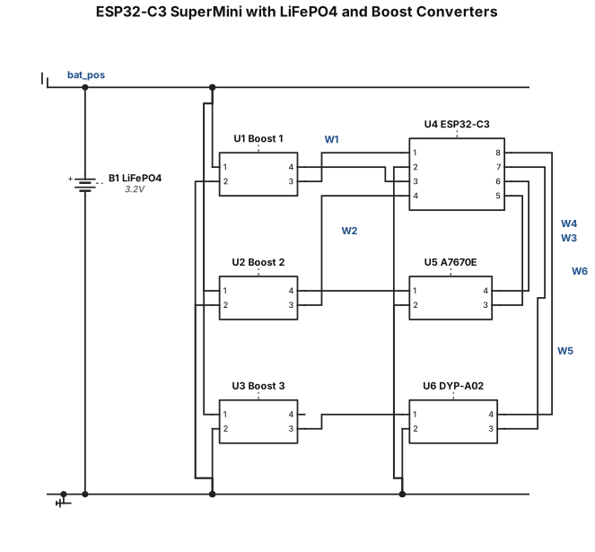
ESP32 C3 SuperMini powered from a 3.2V LiFePO4 battery through a 3.3V boost converter. Battery positive connects to the VIN of three boost converters. GPIO 0 controls Booster 1 EN, GPIO 5 controls Booster 2 EN, GPIO 20 connects directly to A7670E RX, GPIO 21 connects directly to A7670E TX, GPIO 2 connects to DYP-A02 TX, GPIO 3 connects to DYP-A02 RX. All components share a common ground.
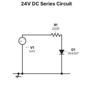
"A clean, standard electrical circuit schematic on a white background. A 24V DC voltage source connected in series with a 2200 Ohm resistor and a 1N4007 silicon diode, ending at a ground connection. Use standard IEEE electronic symbols, crisp black lines, minimalist black-and-white style, no background clutter."
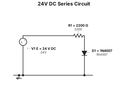
EDIT THE PREVIOUS SCHEMATIC. DO NOT CREATE A NEW CIRCUIT. Keep exactly the same circuit topology, but simplify it to ONLY these components: 1. One DC voltage source: E = 24 V DC 2. One resistor: R1 = 2200 Ω 3. One silicon diode: D1 = 1N4007 4. One GND symbol The ONLY electrical path must be: +24 V DC source -> R1 2200 Ω -> D1 1N4007 -> negative terminal of the same 24 V source. IMPORTANT: - REMOVE the current source I1 completely. - REMOVE all additional voltage/current sources. - REMOVE all extra wires that create parallel branches. - REMOVE labels such as "vplus", "anode", "10.59mA" if they are not part of the standard schematic. - Do not add any capacitor, lamp, switch, fuse, second diode, or second circuit. - Keep exactly ONE source, ONE resistor, and ONE diode. - The diode must be forward biased. - Use standard electrical schematic symbols. - Make the final schematic clean, simple and suitable for a university laboratory report. Show only these component labels: E = 24 V DC R1 = 2200 Ω D1 = 1N4007 Optionally show: I ≈ 10.59 mA U_D = 0.7 V P_D ≈ 7.41 mW
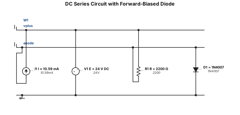
Generate EXACTLY ONE electrical schematic. Do not generate multiple circuits, alternative versions, examples, or additional diagrams. This is for laboratory assignment, option 5. Create ONLY this single DC circuit: 24 V DC voltage source E = 24 V connected in series to R = 2200 ohms resistor connected in series to D1 = 1N4007 silicon diode connected back to the negative terminal of the 24 V source. Circuit topology must be exactly: +24 V DC source -> R1 2200 ohm -> D1 1N4007 -> negative terminal of source. The diode must be FORWARD BIASED: the positive terminal of the 24 V source connects through the resistor to the ANODE of D1; the CATHODE of D1 connects to the negative terminal of the source. Use standard IEC/electrical schematic symbols. Show: - voltage source labeled "E = 24 V DC" - resistor labeled "R = 2200 Ω" - diode labeled "D1 = 1N4007" - ground symbol connected to the negative terminal if appropriate - current direction arrow labeled "I" - diode voltage label "U_D = 0.7 V" - current label "I ≈ 10.59 mA" - diode power label "P_D ≈ 7.41 mW" IMPORTANT: - EXACTLY ONE circuit only - ONLY one voltage source - ONLY one resistor - ONLY one diode - NO bridge rectifier - NO four diodes - NO capacitor - NO lamp - NO switch - NO fuse - NO AC source - NO second circuit - NO alternative circuit - NO additional components - NO decorative electrical diagrams The final result must be a single clean horizontal textbook-style schematic on a white background, suitable for inserting into a university laboratory report.
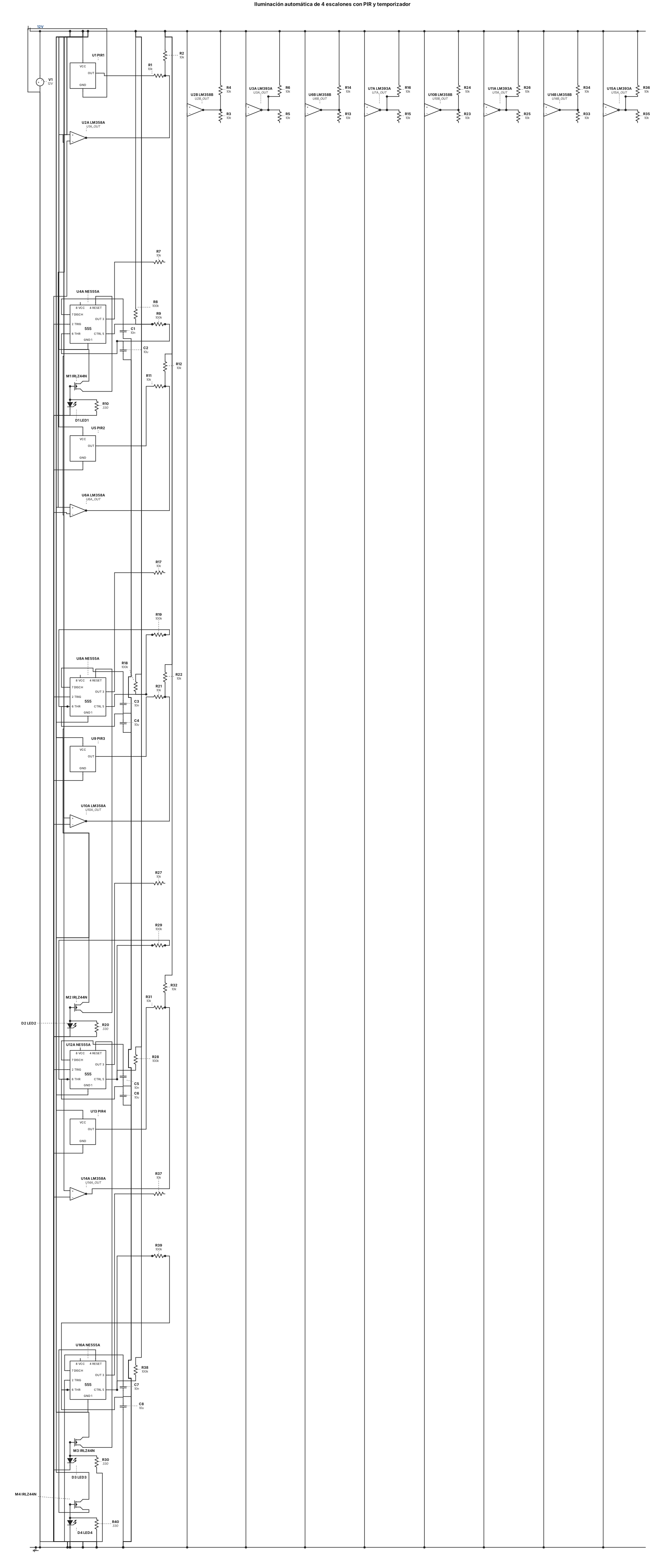
Diseña un sistema de iluminación automática para 4 escalones usando una fuente de 12 V. Cada escalón debe tener un sensor PIR HC-SR501 independiente y una tira LED independiente. Utilizar LM358 para acondicionamiento de señal, LM393 como comparador, NE555 como temporizador e IRLZ44N para controlar cada tira LED. No utilizar Arduino, microcontroladores ni PLC. Todos los canales deben compartir la alimentación de 12 V y GND