Draw the circuit diagram of Seven – Segment Decoder ( 0 - 7 )
NODE ARCHIVE · REAL DIAGRAM BRIEFS
Diagram Examples from Real Visitor Prompts
Browse eligible diagrams shared by FreeDiagram visitors, inspect the exact prompts, and build your own version.
Browse 3262 real creationsCOMMUNITY OUTPUTS · EXACT PROMPTS
Logic Gate
Showing 169–192 of 288. No stock examples or system defaults. Choose a tool, study a real result, then reopen its prompt as your starting point.
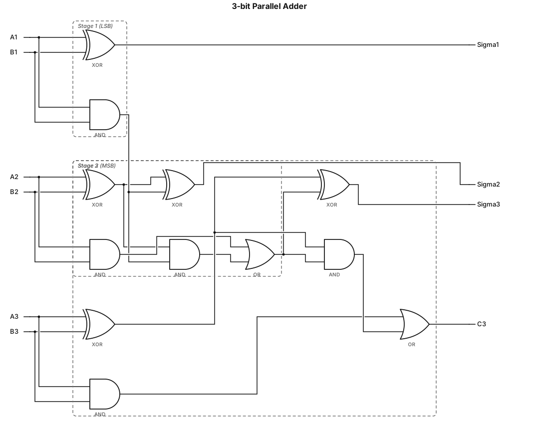
Logic ExpressionsFor a 3-bit parallel adder adding $A = A_3A_2A_1$ and $B = B_3B_2B_1$:Bit 1 (Stage 1 - Half Adder or Full Adder with $C_0 = 0$):$\Sigma_1 = A_1 \oplus B_1$$C_1 = A_1 B_1$Bit 2 (Stage 2 - Full Adder):$\Sigma_2 = A_2 \oplus B_2 \oplus C_1$$C_2 = A_2 B_2 + (A_2 \oplus B_2)C_1$Bit 3 (Stage 3 - Full Adder / MSB):$\Sigma_3 = A_3 \oplus B_3 \oplus C_2$$C_3 = A_3 B_3 + (A_3 \oplus B_3)C_2$Logic Diagram StructureA 3-bit parallel adder is constructed by cascading one half adder (or full adder with grounded carry-in) and two full adders:Stage 1 (LSB): Takes inputs $A_1$ and $B_1$, feeds them into an XOR gate to produce $\Sigma_1$, and an AND gate to produce carry $C_1$.Stage 2: Takes inputs $A_2$, $B_2$, and carry $C_1$, processing them through a Full Adder to yield sum $\Sigma_2$ and carry $C_2$.Stage 3 (MSB): Takes inputs $A_3$, $B_3$, and carry $C_2$ through a final Full Adder to generate sum $\Sigma_3$ and the final carry-out $C_3$.
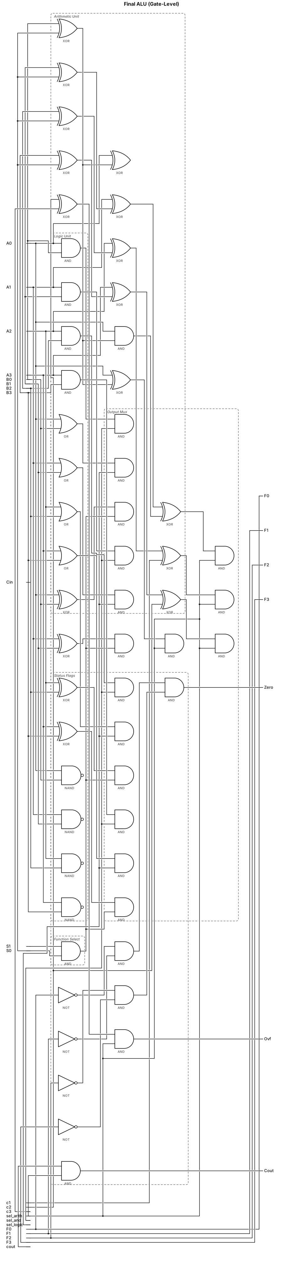
Gate-level schematic for the final ALU design
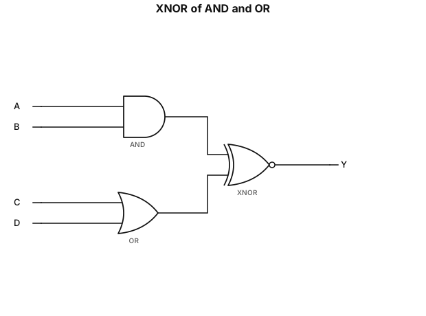
A ───────┐ │ AND ──┐ B ───────┘ │ │ XNOR ──┐ C ───────┐ │ │ │ OR ───┘ │ D ───────┘ │ │ Y
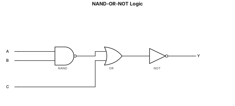
A ───────┐ │ NAND ──┐ B ───────┘ │ │ OR ── NOT ── Y C ─────────────────┘
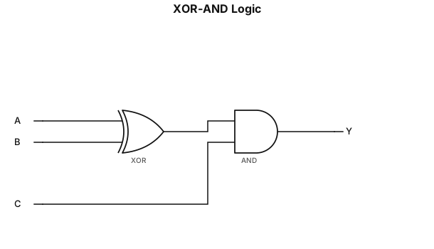
A ───────┐ │ XOR ──┐ B ───────┘ │ │ AND ─── Y C ───────────────┘
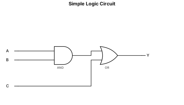
A ───────┐ │ AND ──┐ B ───────┘ │ │ OR ─── Y C ───────────────┘
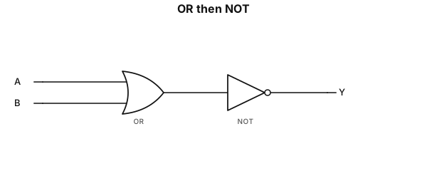
A ───────┐ │ OR ── NOT ── Y B ───────┘
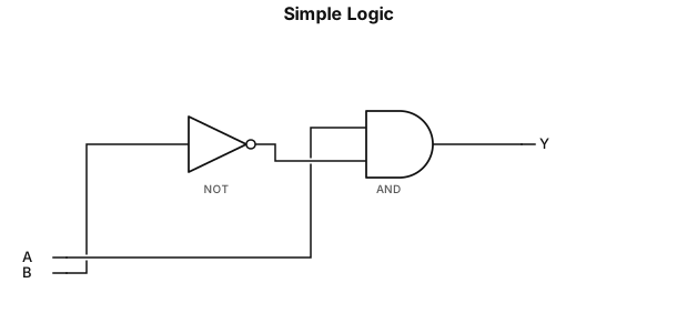
A ───────┐ │ AND ─── Y B ── NOT ┘
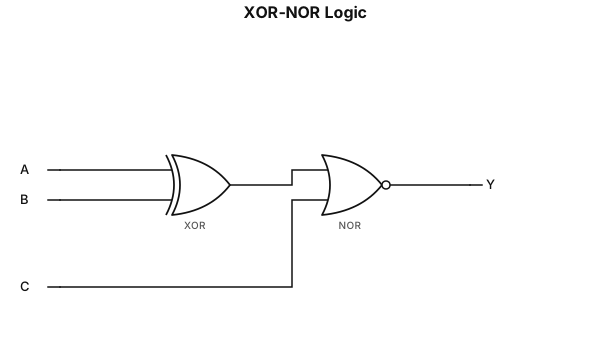
A ───────┐ │ XOR ──┐ B ───────┘ │ │ NOR ─── Y C ───────────────┘
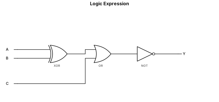
Y = [(A ⊕ B) + C]'
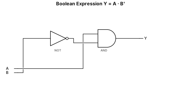
Y = A · B'
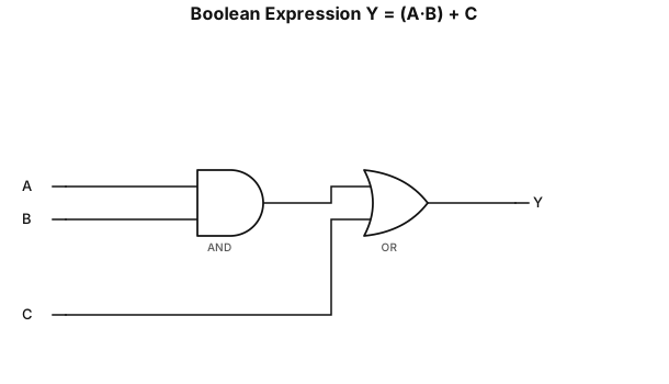
Y = (A · B) + C
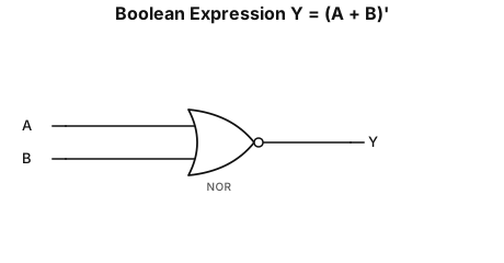
Boolean expression: Y = (A + B)'
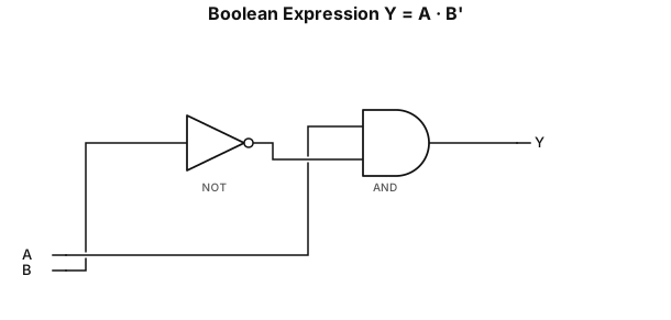
Boolean expression: Y = A · B'
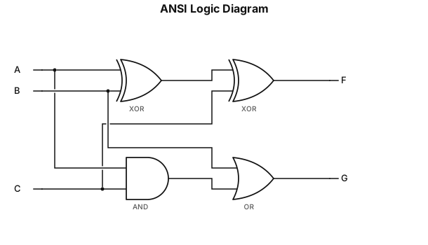
ANSI standard logic diagram. Inputs A,B,C on left, outputs F,G on right. XOR‑1: inputs A and B. XOR‑2: first input = output of XOR‑1, second input = signal C. Output of XOR‑2 is F. NO WIRE FROM B TO XOR‑2. AND gate: inputs A and C. OR gate: inputs B and output of AND gate. Output of OR gate is G. Black filled dots on all wire‑branch points. No extra boxes, only labels A B C F G.
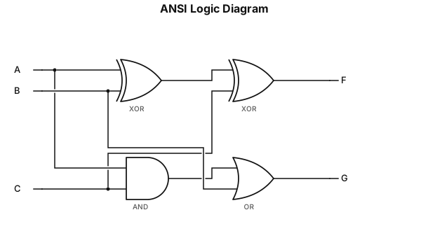
ANSI logic gate diagram.Inputs:A,B,C left side.Outputs:F,G right side. Gate1:XOR,input1=A,input2=B. Gate2:XOR,input1=output of Gate1,input2=C. Gate2 output=F. Do NOT connect B to Gate2. Gate3:AND,input1=A,input2=C. Gate4:OR,input1=output of Gate3,input2=B. Gate4 output=G. Add black filled junction dots at every wire split.Standard shape ANSI gates.No text box,only simple labels A B C F G.
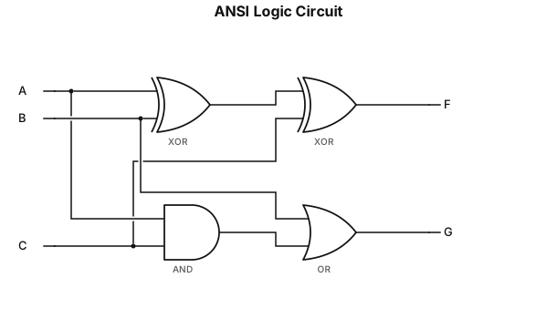
Draw ANSI standard logic circuit diagram. Three inputs A, B, C on left side. Two outputs F and G on right side. F = (A XOR B) XOR C: First XOR gate inputs A and B. Output of first XOR connects to top input pin of second XOR gate. Signal C connects to bottom input pin of second XOR gate. Second XOR gate outputs F. G = B OR (A AND C): AND gate inputs A and C. Output of AND gate and signal B go into OR gate. OR gate outputs G. Draw filled black solid junction dots at every wire split node. Use standard distinctive‑shape ANSI gate symbols. Label outputs simply F and G, no boxes.
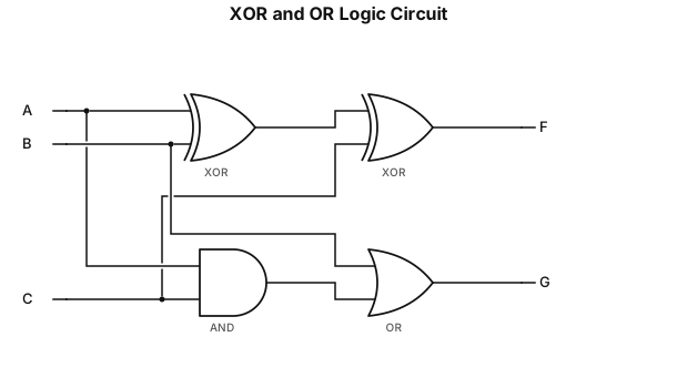
Standard ANSI logic gate schematic. Left inputs A,B,C. Right outputs F and G. F path: First XOR gate inputs A and B. Output of first XOR connects to the top‑input of second XOR gate. Signal C connects to bottom‑input of second XOR gate. Output of second XOR=F. F=(A xor B) xor C. G path: AND gate inputs A and C. AND output and signal B feed into OR gate. OR output=G. G = B OR (A AND C). Draw filled black dot junctions on every wire split point. Do NOT feed B into the second XOR gate.
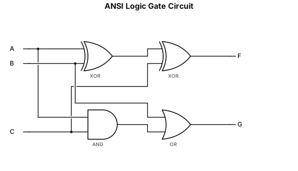
绘制标准ANSI逻辑门电路图,左侧3个共用输入A,B,C,右侧两个输出F、G。 F支路:两级级联异或门,第一个XOR输入A、B,输出接到第二个XOR;第二个XOR另一个输入C,输出F,F=(A⊕B)⊕C。 G支路:一个与门AND输入A、C,AND输出和B送入或门OR,OR输出G,G=B+(A·C)。 导线分叉位置画上实心黑色连接圆点,使用课本标准异形逻辑门符号。
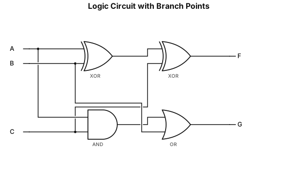
1. 输入:A,B,C 2.F 通路: - XOR1 输入 A、B;XOR1 输出接 XOR2 输入 1;XOR2 输入 2 接 C;XOR2 输出 = F 3.G 通路: - AND 输入 A、C;AND 输出接 OR 输入 1;OR 输入 2 接 B;OR 输出 = G 4. 导线分叉处自动出现**实心黑点**,就是题目要求的分叉标记。
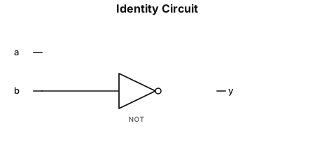
A logic gate circuit with 2 input lines (a and b) and one output line and the output line = 1 if and only is line a = 1 (use AND, OR, and NOT gates)
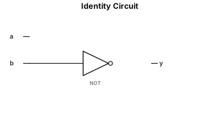
A logic gate circuit with 2 input lines (a and b) and one output line and the output line = 1 if and only is line a = 1 (use And, OR, and NOT gates)
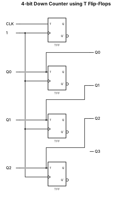
Design and set up a 4-bit down counter using T-flip flop