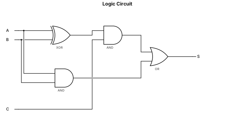
S=(A⊕B)C+AB using 2 input gates
NODE ARCHIVE · REAL DIAGRAM BRIEFS
Diagram Examples from Real Visitor Prompts
Browse eligible diagrams shared by FreeDiagram visitors, inspect the exact prompts, and build your own version.
Browse 3266 real creationsCOMMUNITY OUTPUTS · EXACT PROMPTS
All visitor creations
Showing 313–336 of 3266. No stock examples or system defaults. Choose a tool, study a real result, then reopen its prompt as your starting point.
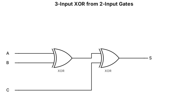
S=A⊕B⊕C using 2 input gates
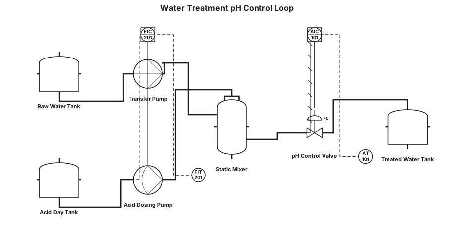
Water treatment loop with pH control and dosing pump
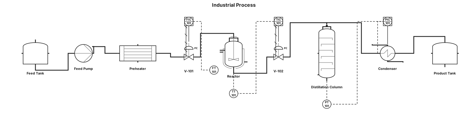
A P&ID for an industrial process
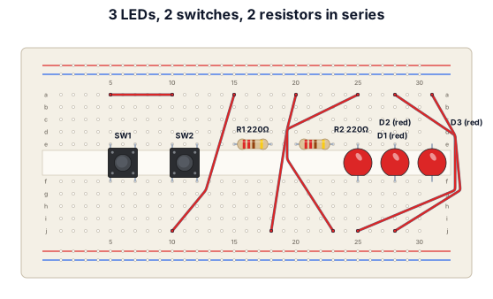
a breadboard of 3 leds two stwict 2 ereistor connected in series use only 3 wieres

meta ad and performance marketing
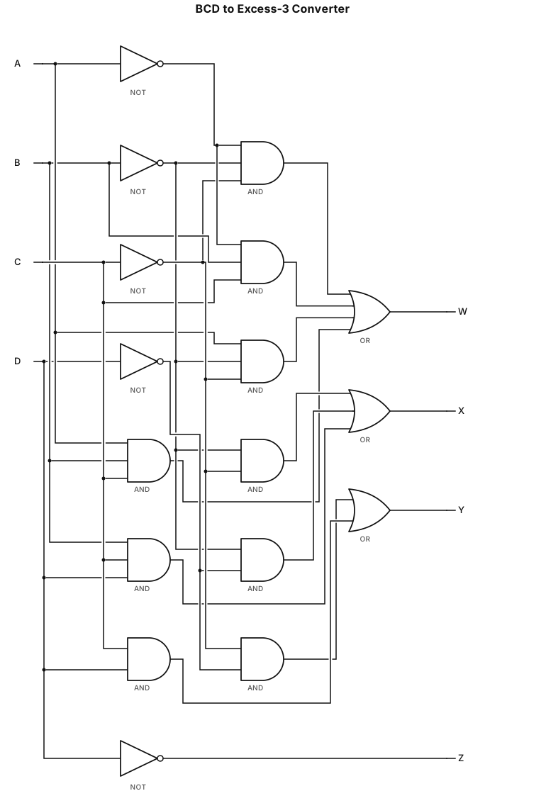
bcd to excess 3 ,inputs ABCD outputs WXYZ
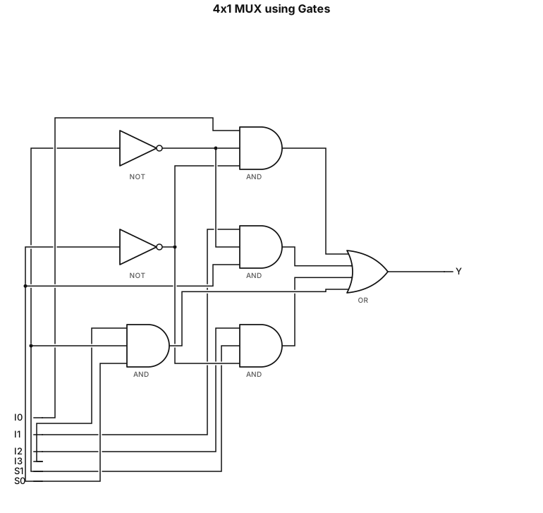
Implement 4x1 MUX using gates,S1,S0 are select lines ,I0,I1,I2,I3 are inputs,Y is output
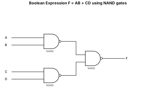
3) Implement a given Boolean expression using only NAND gates:F=AB+CD
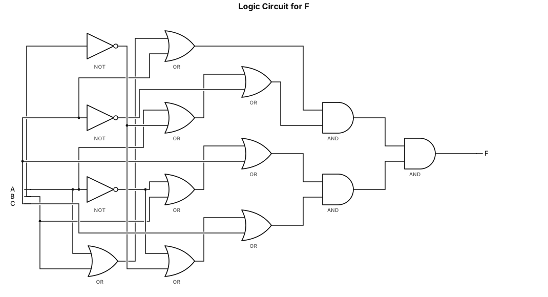
Draw the logic circuit diagram for (F=(A+B+C)(A+B'+C')(A'+B+C)(A'+B'+C) ), Strictly using less than or equal to 2 input gates Inputs A,B,C;output F.
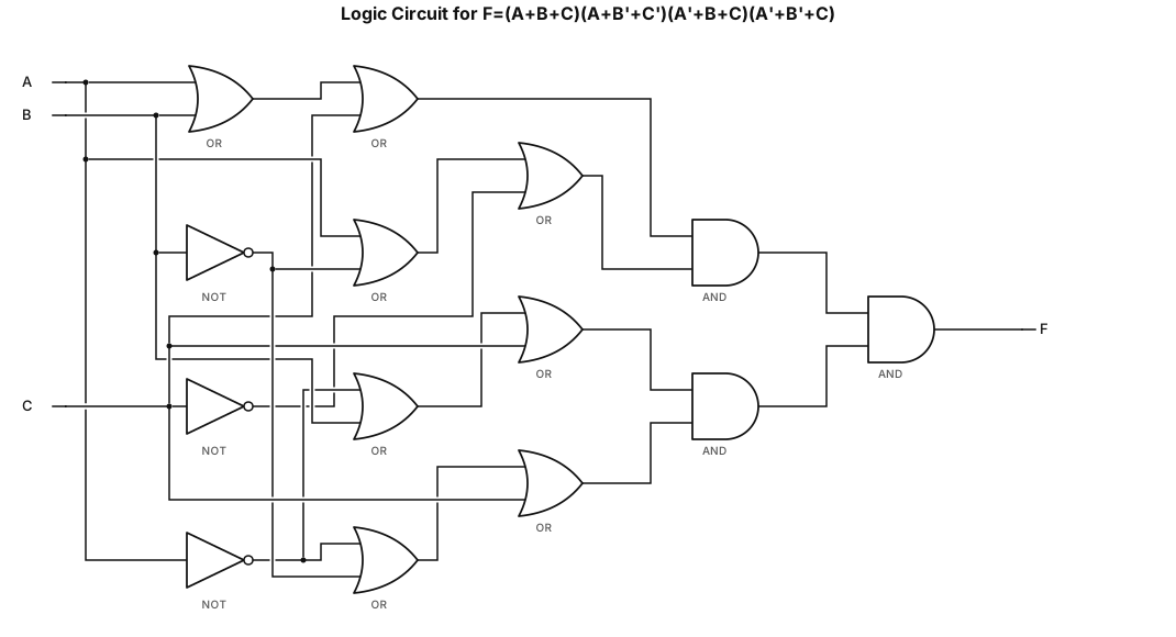
Draw the logic circuit diagram for (F=(A+B+C)(A+B'+C')(A'+B+C)(A'+B'+C) ), Strictly using less than or equal to 2 input gatesInputs A,B,C,D; output F.
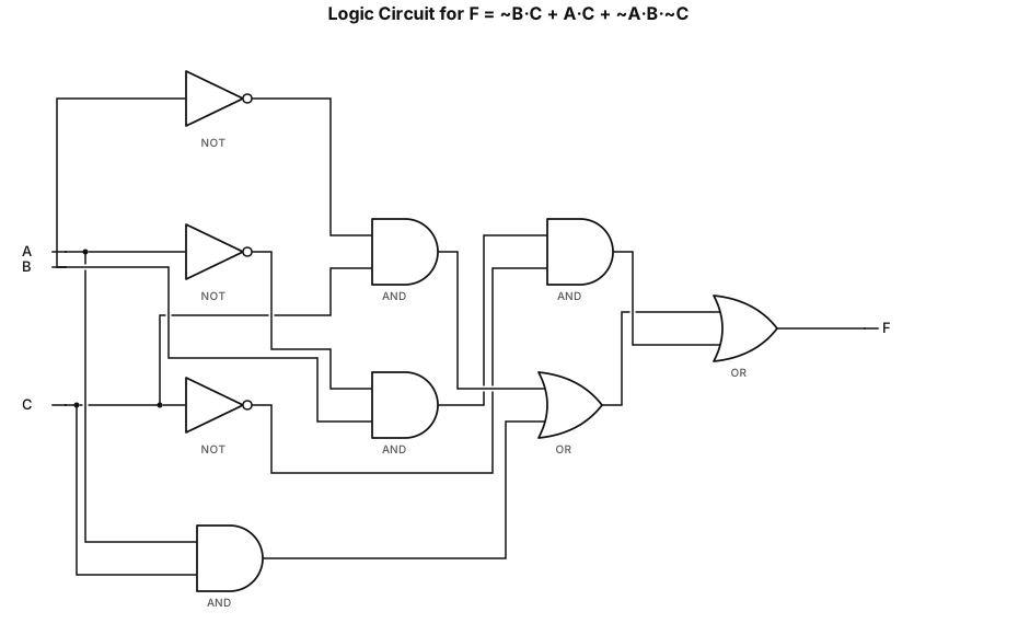
Draw the logic circuit diagram for (F=¯B C+AC+¯A B¯C), Strictly using less than or equal to 2 input gatesInputs A,B,C,D; output F.
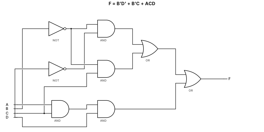
Draw the logic circuit diagram for F = B̅ D̅ + B̅ C + ACD, Strictly using less than or equal to 2 input gatesInputs A,B,C,D; output F.
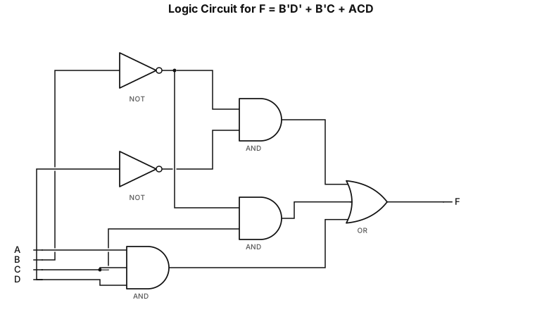
Draw the logic circuit diagram for F = B̅ D̅ + B̅ C + ACD, Inputs A,B,C,D; output F.
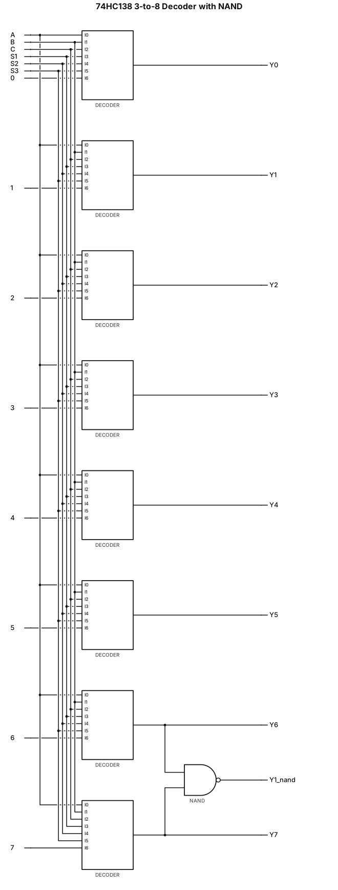
One single 74HC138 3-to-8 decoder. A2,A1,A0 = A,B,C. S1=1, S2=0, S3=0. Only one 2-input NAND gate, inputs connect to Y6 and Y7 of this decoder, output Y1. Standard IEEE logic symbols, clean wires, exam style.
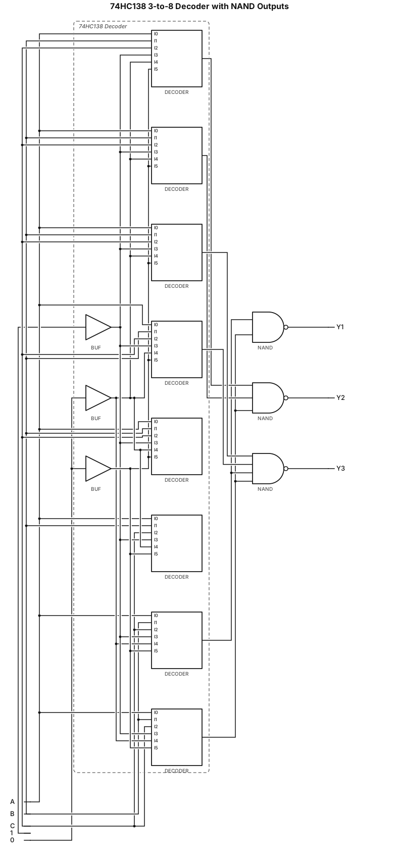
Digital logic circuit, ONLY ONE 74HC138 3-to-8 decoder chip. Address pins A2,A1,A0 connect to A,B,C. Enable S1=1, S2=0, S3=0. There are three NAND gates connected to the output of this single decoder: 2-input NAND: inputs Y6,Y7, output Y1 3-input NAND: inputs Y0,Y1,Y7, output Y2 4-input NAND: inputs Y2,Y3,Y6,Y7, output Y3 Standard IEEE symbols, white background, clean orthogonal wires, label all pins, for digital electronics exam
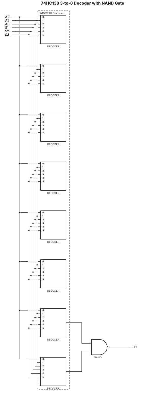
Digital logic circuit with 74HC138 3-to-8 decoder. Address pins A2,A1,A0 connect to A,B,C. Enable S1=1, S2=0, S3=0. 2-input NAND gate, inputs Y6,Y7, output Y1. Standard IEEE symbols, white background, clean orthogonal wires, label all pins, for digital electronics exam
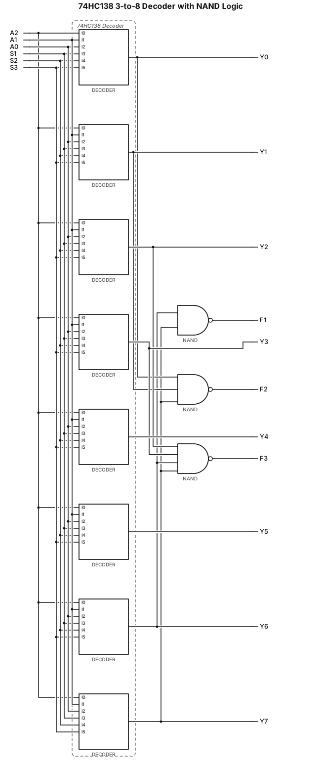
Digital logic circuit with 74HC138 3-to-8 decoder. Address pins A2,A1,A0 connect to A,B,C. Enable S1=1, S2=0, S3=0. Three NAND gates: 2-input NAND: inputs Y6,Y7, output Y1 3-input NAND: inputs Y0,Y1,Y7, output Y2 4-input NAND: inputs Y2,Y3,Y6,Y7, output Y3 Standard IEEE symbols, white background, clean orthogonal wires, label all pins, for digital electronics exam
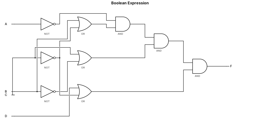
A'(B + C')(C + B')(D + C')
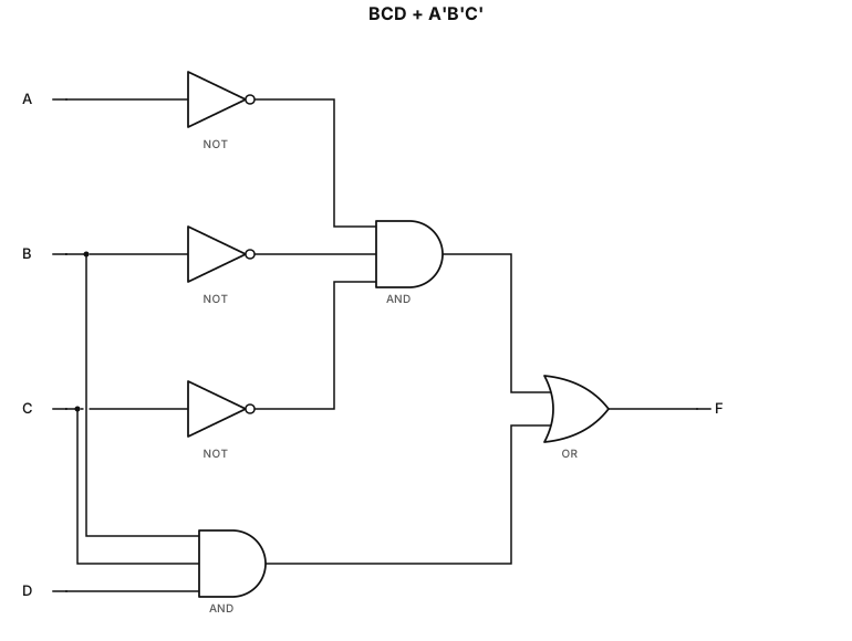
(BCD) + (A'B'C')
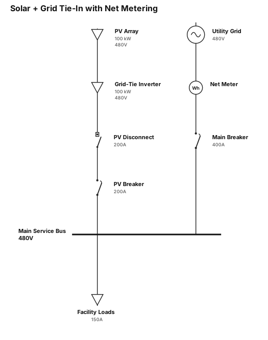
Solar plus grid tie-in with inverter and net metering disconnect
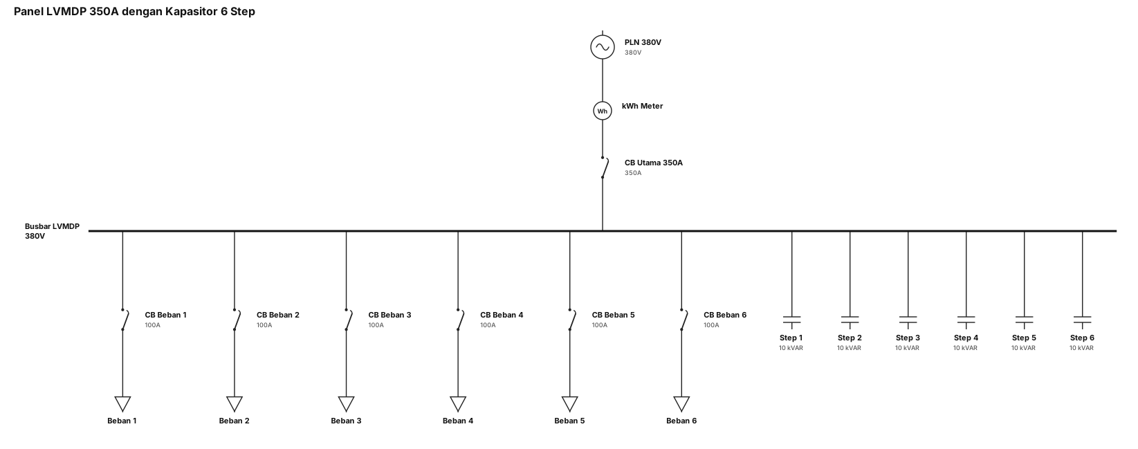
Buatkan singel line diagram untuk panel LVMDP kapasitas 350 Ampere dengan kapasitor 6 step cosphi 9,5
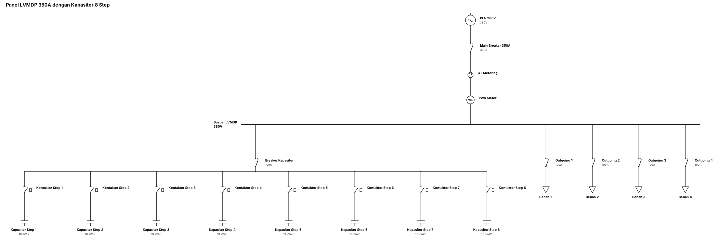
Buatkan singel line diagram untuk panel LVMDP kapasitas 350 Ampere dengan kapasitor 8 step
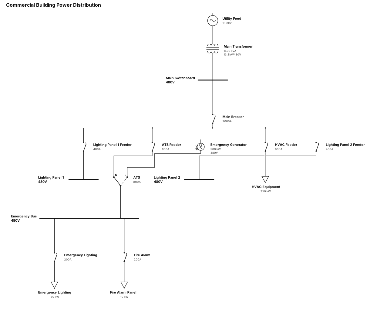
A single-line diagram for a commercial building: utility feed through a main transformer to a 480V switchboard, then to lighting panels, HVAC equipment, and an emergency generator with ATS