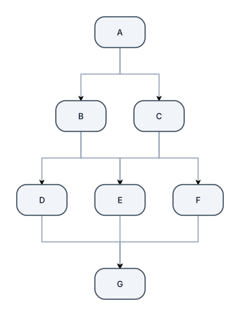
→ A → B → D → G → ↘ E ↗ A → C → E y C → F → G
NODE ARCHIVE · REAL DIAGRAM BRIEFS
Diagram Examples from Real Visitor Prompts
Browse eligible diagrams shared by FreeDiagram visitors, inspect the exact prompts, and build your own version.
Browse 3261 real creationsCOMMUNITY OUTPUTS · EXACT PROMPTS
All visitor creations
Showing 25–48 of 3261. No stock examples or system defaults. Choose a tool, study a real result, then reopen its prompt as your starting point.
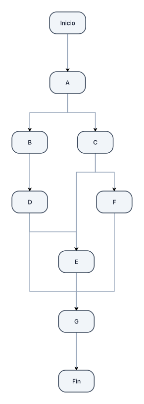
Inicio → A → B → D → G → Fin ↘ E ↗ A → C → E y C → F → G

Haz un flujograma de como prepar un sandwich INICIO -> ¿Hay pan e ingredientes? - SI -> Lavar vegetales (lechuga y tomate) - NO -> Comprar ingredientes necesarios -> Regresar a casa -> Lavar vegetales (lechuga y tomate) Lavar vegetales -> Cortar tomate en rodajas y secar la lechuga Cortar tomate -> Colocar la primera rebanada de pan en la tabla o plato Colocar primera rebanada -> ¿Quieres untar algo (mayonesa, mantequilla)? - SI -> Untar en ambas rebanadas -> Poner hoja de lechuga sobre la primera rebanada - NO -> Poner hoja de lechuga sobre la primera rebanada Poner hoja de lechuga -> Colocar rodajas de tomate sobre la lechuga Colocar rodajas de tomate -> Añadir láminas de jamón dobladas Añadir jamón -> Agregar las láminas de queso Agregar queso -> Colocar la segunda rebanada de pan (tapa superior) Colocar segunda rebanada -> ¿Prefieres el sándwich caliente? - SI -> Tostar en sartén o plancha -> Cortar a la mitad (en diagonal) - NO -> Cortar a la mitad (en diagonal) Cortar a la mitad -> FIN
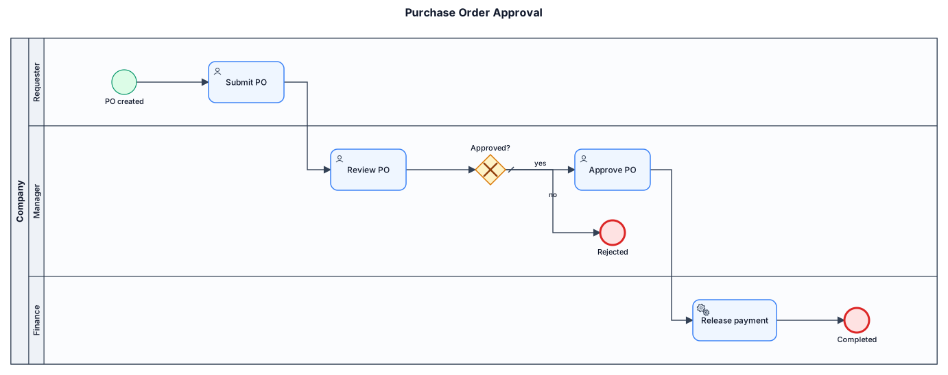
A BPMN diagram of a purchase-order approval process across three lanes: requester submits a PO, manager reviews and approves or rejects, finance releases payment
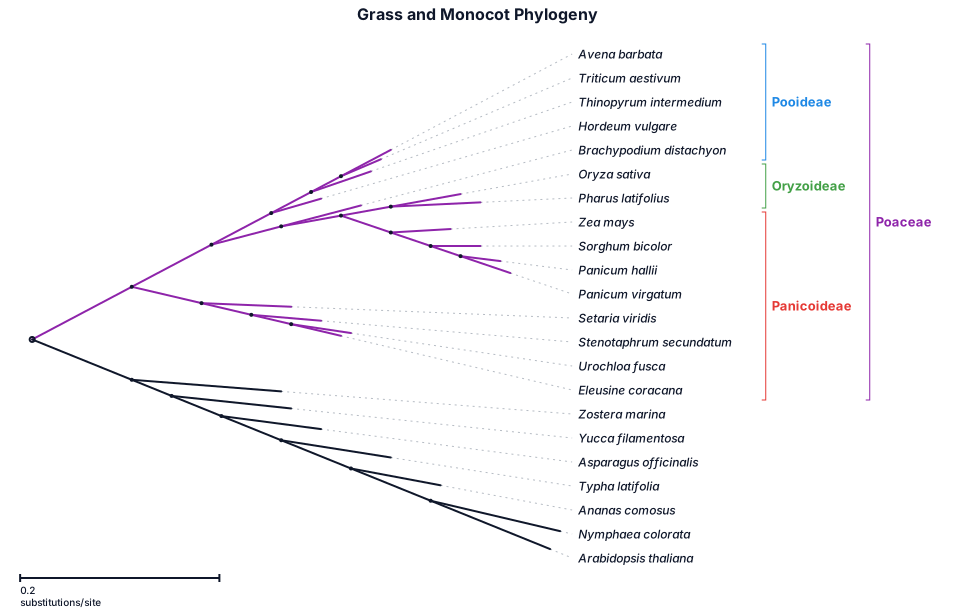
Avena barbata Eleusine coracana Hordeum vulgare Oryza sativa Pharus latifolius Thinopyrum intermedium Triticum aestivum Brachypodium distachyon Panicum virgatum Setaria viridis Stenotaphrum secundatum Urochloa fusca Zea mays Panicum hallii Sorghum bicolor Zostera marina Yucca filamentosa Typha latifolia Asparagus officinalis Ananas comosus Arabidopsis thaliana Nymphaea colorata
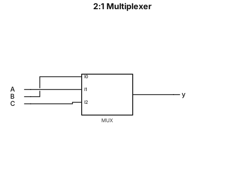
Draw MUX Circuit (Exact Diagram Style) Please draw a 2:1 Multiplexer circuit diagram matching the exact visual symbol and style from the textbook assignment: MUX Symbol Shape: Draw a vertical, narrow trapezoid shape for the MUX block. Inside the block, write 1 at the top input level and 0 at the bottom input level. Signal Connections & Labels: Top Input: Draw an arrow pointing from the left into port 1 and label it B. Bottom Input: Draw an arrow pointing from the left into port 0 and label it A. Select Input: Draw an arrow pointing directly UP into the bottom base of the trapezoid and label it C. Output: Draw an arrow pointing to the right coming out of the center-right side and label it y. Visual Style: Replicate the exact layout from the task image: clean black lines on a white background. Keep all text labels (A, B, C, y, 1, 0) clearly placed next to their respective arrows.
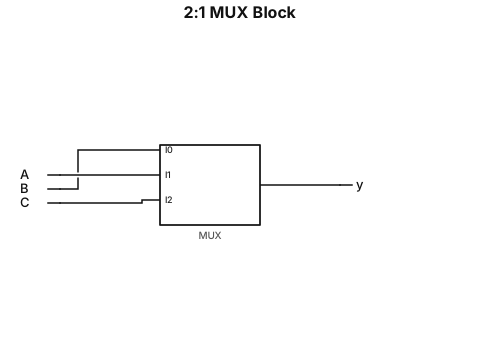
Draw MUX Block CircuitPlease generate a visual circuit schematic of a 2-to-1 Multiplexer (2:1 MUX) based on the following specifications:MUX Block Representation:Draw a standard trapezoidal or rectangular 2:1 MUX component block.Label the inside of the block clearly with 2:1 MUX.Mark the two left-side input ports as 1 (top) and 0 (bottom).Connecting Signals:Select line ($s$): Draw an arrow entering the bottom of the MUX block and label it C.Top input (1): Draw an arrow coming from the left into port 1 and label it B.Bottom input (0): Draw an arrow coming from the left into port 0 and label it A.Output ($y$): Draw an arrow exiting from the right side of the MUX block and label it y.Formatting & Visual Style:Keep the design clean, minimalist, and easy to read.Ensure all wire connections and text labels (A, B, C, y, 0, 1) are clearly separated without overlapping lines.
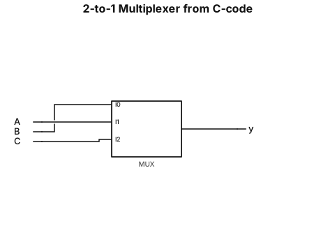
Draw MUX Circuit from C-codePlease draw a clear and clean circuit diagram of a 2-to-1 Multiplexer (2:1 MUX) implementing the following C-code logic:Cif (C == 0) { y = A; } else { y = B; } Layout and Labeling Instructions:MUX Symbol:Draw a standard trapezoidal 2:1 MUX block.Mark the upper data input as 1 and the lower data input as 0.Pin Connections:Select Line ($s$): Connect the input variable C to the select input at the bottom of the MUX.Data Input 1: Connect the input variable B to the upper data input (labeled 1).Data Input 0: Connect the input variable A to the lower data input (labeled 0).Output: Label the right-side output line as y.Visual Style:Keep all signal lines straight, well-spaced, and cleanly labeled.Ensure there is no overlapping text or cluttered lines.
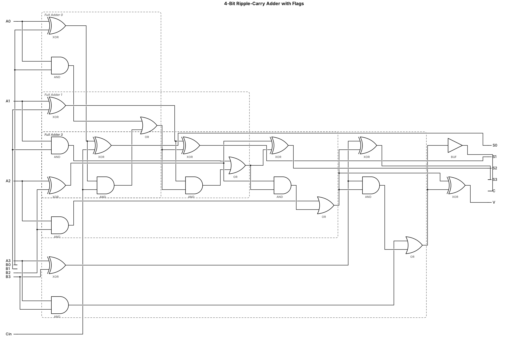
4-Bit Adder Schematic & VisualizationPlease create a clear block diagram or schematic explanation for a 4-bit binary adder circuit based on the following task:Circuit Components:Show a 4-bit ripple-carry adder made by chaining 4 Full Adders together (for bits $0$ to $3$).Clearly label the inputs: first 4-bit number ($A = 1011_2$) and second 4-bit number ($B$ / aaaa or bbbb).Show the input carry ($C_{in}$) and the output sum.Flag Generation Logic:Illustrate how the Carry flag ($C$) is generated from the final carry-out ($C_{out}$).Illustrate how the Overflow flag ($V$) is detected (e.g., using an XOR gate on the carry-in and carry-out of the most significant bit, $C_3 \oplus C_4$).Visual Layout:Keep the blocks well-separated, use clear data paths for the 4-bit buses, and ensure all labels for bits, sums, and flags ($C$ and $V$) are easy to read.
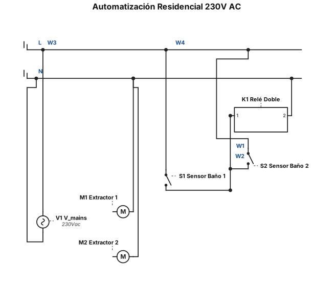
Diseña un esquema eléctrico residencial de automatización a 230V AC. Incluye los siguientes componentes etiquetados: 'Sensor Baño 1', 'Sensor Baño 2', 'Relé Doble' (con bobina A1-A2 y dos contactos independientes NO 1 y NO 2), 'Extractor 1' y 'Extractor 2'. Las salidas de fase de ambos sensores deben conectarse en paralelo al borne A1 de la bobina del relé. El borne A2 va a la línea de Neutro. Conecta la Fase directa a las entradas comunes (COM) de ambos contactos del relé. La salida NO 1 debe alimentar al Extractor 1 y la salida NO 2 debe alimentar al Extractor 2. Conecta el Neutro a todos los componentes."
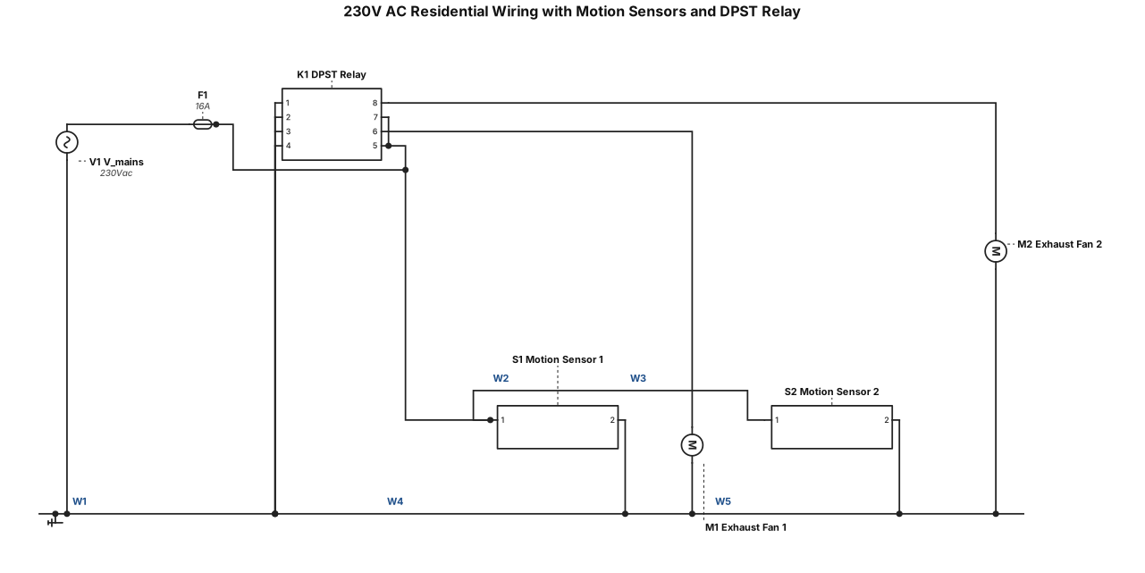
Draw a 230V AC residential wiring diagram. Components: 'Motion Sensor 1', 'Motion Sensor 2', 'DPST Relay' (Double Pole Single Throw relay with coil terminals A1/A2 and two Normally Open contacts), 'Exhaust Fan 1', and 'Exhaust Fan 2'. Connect the switch leg outputs of both Motion Sensor 1 and Motion Sensor 2 in parallel to the relay coil terminal A1. Connect coil terminal A2 to the Neutral line. Connect direct Hot/Line to the common terminals of both relay contacts. Connect contact NO 1 to Exhaust Fan 1, and contact NO 2 to Exhaust Fan 2. Connect Neutral to all components.
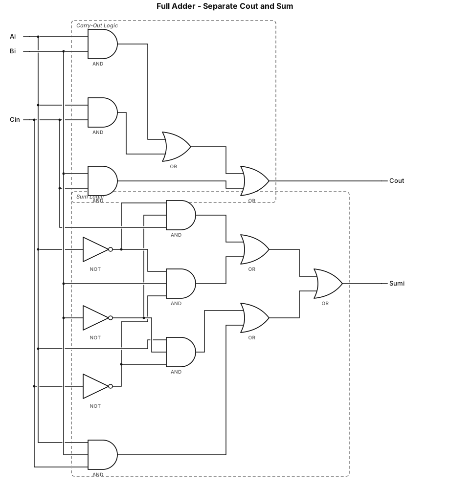
Separate Design for Full Adder ($C_{out}$ and $Sum_i$)Please design the combinational logic gate network for a Full Adder using only AND, OR, and NOT gates. To keep the schematic clean, readable, and well-organized, please design the two outputs completely separately in distinct sections:General Instructions:Use only AND, OR, and NOT gates (no XOR or other prohibited gates).Keep all logic gates well-spaced and separated.Route all connecting wires clearly without unnecessary crossings or clutter.Part 1: Carry-Out ($C_{out}$) Logic NetworkInputs & Output:Inputs: $A_i$, $B_i$, $C_{in}$Output: $C_{out}$Boolean Equation:$$C_{out} = A_i B_i + A_i C_{in} + B_i C_{in}$$Gate Implementation:Use 3 AND gates to compute the product terms: $A_i B_i$, $A_i C_{in}$, and $B_i C_{in}$.Use an OR gate network to combine these three terms into $C_{out}$.Part 2: Sum ($Sum_i$) Logic NetworkInputs & Output:Inputs: $A_i$, $B_i$, $C_{in}$Output: $Sum_i$Boolean Equation:$$Sum_i = \bar{A}_i\bar{B}_iC_{in} + \bar{A}_iB_i\bar{C}_{in} + A_i\bar{B}_i\bar{C}_{in} + A_iB_iC_{in}$$Gate Implementation:Use NOT gates to invert inputs $A_i$, $B_i$, and $C_{in}$ to get $\bar{A}_i$, $\bar{B}_i$, and $\bar{C}_{in}$.Use four 3-input AND gates to compute the four minterms.Use an OR gate network to combine the outputs of the four AND gates into $Sum_i$.Please provide the text-based schematic or connection layout following these separated sections strictly.
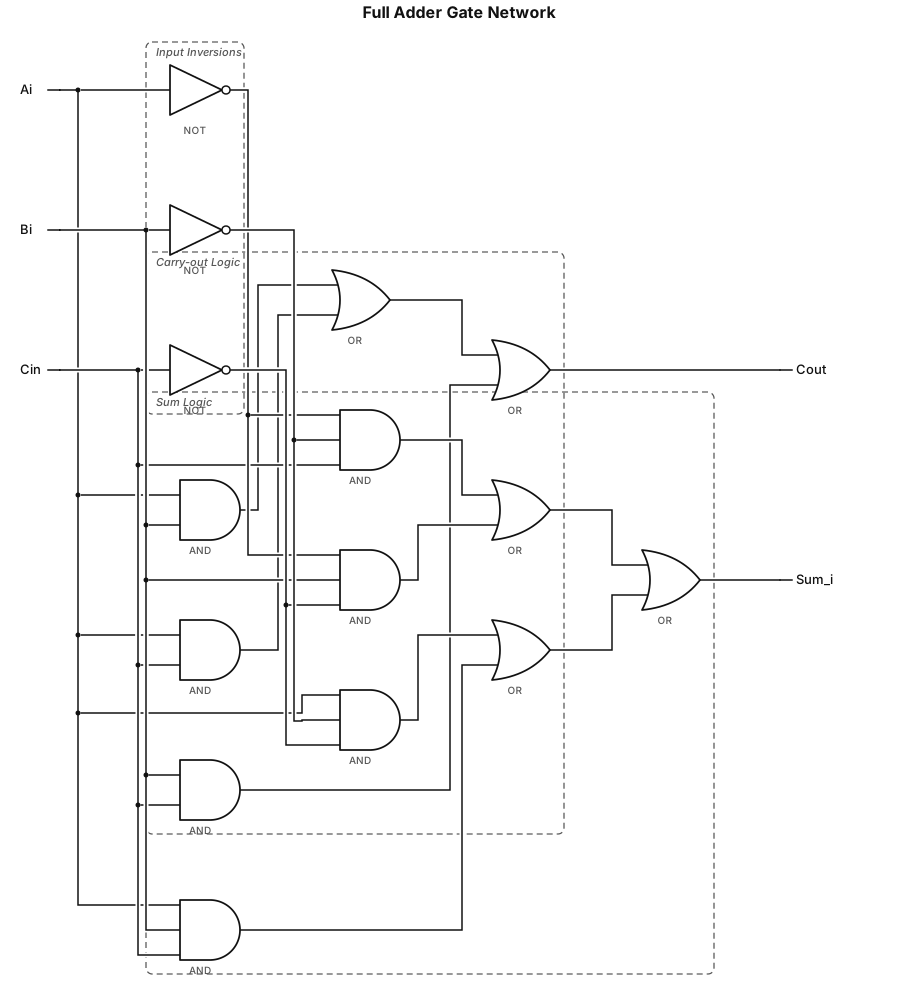
Full Adder Gate Network Implementation (Clean Layout)Please design the combinational logic gate network for a Full Adder ($Sum_i$ and $C_{out}$) using only AND, OR, and NOT gates, based on the following specifications.Important Layout Instructions:Place all logic gates well-separated and spaced out clearly to avoid overlapping or clutter.Route all connecting wires distinctly, keeping them organized and easy to follow without unnecessary crossing.Inputs and Outputs:Inputs: $A_i$, $B_i$, and $C_{in}$ (carry-in)Outputs: $Sum_i$ (sum) and $C_{out}$ (carry-out)Boolean Equations:Carry-out ($C_{out}$):$$C_{out} = A_i B_i + A_i C_{in} + B_i C_{in}$$Sum ($Sum_i$):$$Sum_i = \bar{A}_i\bar{B}_iC_{in} + \bar{A}_iB_i\bar{C}_{in} + A_i\bar{B}_i\bar{C}_{in} + A_iB_iC_{in}$$Gate Network Instructions:For $C_{out}$:Use 3 AND gates to compute the product terms: $A_i B_i$, $A_i C_{in}$, and $B_i C_{in}$.Use an OR gate (or a combination of 2-input OR gates) to sum up these three terms.For $Sum_i$:Use NOT gates to invert inputs $A_i$, $B_i$, and $C_{in}$ to get $\bar{A}_i$, $\bar{B}_i$, and $\bar{C}_{in}$.Use four 3-input AND gates to compute the four minterms: $\bar{A}_i\bar{B}_iC_{in}$, $\bar{A}_iB_i\bar{C}_{in}$, $A_i\bar{B}_i\bar{C}_{in}$, and $A_iB_iC_{in}$.Use an OR gate network to combine the outputs of these four AND gates into $Sum_i$.Please provide a clean, well-spaced connection layout or text-based schematic description following these rules strictly without using XOR or other prohibited gates.
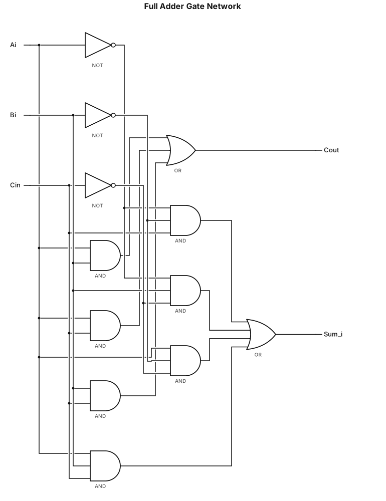
Full Adder Gate Network ImplementationPlease design the combinational logic gate network for a Full Adder ($Sum_i$ and $C_{out}$) using only AND, OR, and NOT gates, based on the following specifications:Inputs and Outputs:Inputs: $A_i$, $B_i$, and $C_{in}$ (carry-in)Outputs: $Sum_i$ (sum) and $C_{out}$ (carry-out)Boolean Equations:Carry-out ($C_{out}$):$$C_{out} = A_i B_i + A_i C_{in} + B_i C_{in}$$Sum ($Sum_i$):$$Sum_i = \bar{A}_i\bar{B}_iC_{in} + \bar{A}_iB_i\bar{C}_{in} + A_i\bar{B}_i\bar{C}_{in} + A_iB_iC_{in}$$Gate Network Instructions:For $C_{out}$:Use 3 AND gates to compute the product terms: $A_i B_i$, $A_i C_{in}$, and $B_i C_{in}$.Use an OR gate (or a combination of 2-input OR gates) to sum up these three terms.For $Sum_i$:Use NOT gates to invert inputs $A_i$, $B_i$, and $C_{in}$ to get $\bar{A}_i$, $\bar{B}_i$, and $\bar{C}_{in}$.Use four 3-input AND gates to compute the four minterms: $\bar{A}_i\bar{B}_iC_{in}$, $\bar{A}_iB_i\bar{C}_{in}$, $A_i\bar{B}_i\bar{C}_{in}$, and $A_iB_iC_{in}$.Use an OR gate network to combine the outputs of these four AND gates into $Sum_i$.Please provide the detailed connection layout or schematic description following these rules strictly without using XOR or other prohibited gates. make the ports be apart from each other the way that its clear and dont make the routes so tangeled
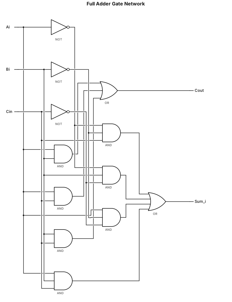
Full Adder Gate Network ImplementationPlease design the combinational logic gate network for a Full Adder ($Sum_i$ and $C_{out}$) using only AND, OR, and NOT gates, based on the following specifications:Inputs and Outputs:Inputs: $A_i$, $B_i$, and $C_{in}$ (carry-in)Outputs: $Sum_i$ (sum) and $C_{out}$ (carry-out)Boolean Equations:Carry-out ($C_{out}$):$$C_{out} = A_i B_i + A_i C_{in} + B_i C_{in}$$Sum ($Sum_i$):$$Sum_i = \bar{A}_i\bar{B}_iC_{in} + \bar{A}_iB_i\bar{C}_{in} + A_i\bar{B}_i\bar{C}_{in} + A_iB_iC_{in}$$Gate Network Instructions:For $C_{out}$:Use 3 AND gates to compute the product terms: $A_i B_i$, $A_i C_{in}$, and $B_i C_{in}$.Use an OR gate (or a combination of 2-input OR gates) to sum up these three terms.For $Sum_i$:Use NOT gates to invert inputs $A_i$, $B_i$, and $C_{in}$ to get $\bar{A}_i$, $\bar{B}_i$, and $\bar{C}_{in}$.Use four 3-input AND gates to compute the four minterms: $\bar{A}_i\bar{B}_iC_{in}$, $\bar{A}_iB_i\bar{C}_{in}$, $A_i\bar{B}_i\bar{C}_{in}$, and $A_iB_iC_{in}$.Use an OR gate network to combine the outputs of these four AND gates into $Sum_i$.Please provide the detailed connection layout or schematic description following these rules strictly without using XOR or other prohibited gates. and dont do it so close together
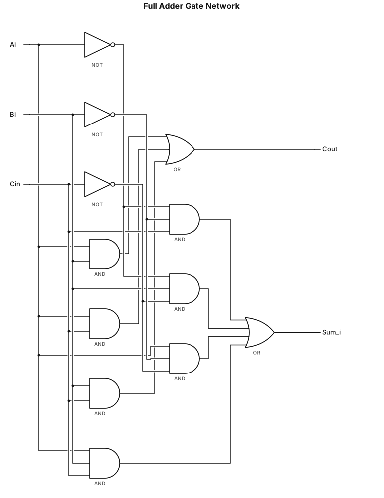
Full Adder Gate Network ImplementationPlease design the combinational logic gate network for a Full Adder ($Sum_i$ and $C_{out}$) using only AND, OR, and NOT gates, based on the following specifications:Inputs and Outputs:Inputs: $A_i$, $B_i$, and $C_{in}$ (carry-in)Outputs: $Sum_i$ (sum) and $C_{out}$ (carry-out)Boolean Equations:Carry-out ($C_{out}$):$$C_{out} = A_i B_i + A_i C_{in} + B_i C_{in}$$Sum ($Sum_i$):$$Sum_i = \bar{A}_i\bar{B}_iC_{in} + \bar{A}_iB_i\bar{C}_{in} + A_i\bar{B}_i\bar{C}_{in} + A_iB_iC_{in}$$Gate Network Instructions:For $C_{out}$:Use 3 AND gates to compute the product terms: $A_i B_i$, $A_i C_{in}$, and $B_i C_{in}$.Use an OR gate (or a combination of 2-input OR gates) to sum up these three terms.For $Sum_i$:Use NOT gates to invert inputs $A_i$, $B_i$, and $C_{in}$ to get $\bar{A}_i$, $\bar{B}_i$, and $\bar{C}_{in}$.Use four 3-input AND gates to compute the four minterms: $\bar{A}_i\bar{B}_iC_{in}$, $\bar{A}_iB_i\bar{C}_{in}$, $A_i\bar{B}_i\bar{C}_{in}$, and $A_iB_iC_{in}$.Use an OR gate network to combine the outputs of these four AND gates into $Sum_i$.Please provide the detailed connection layout or schematic description following these rules strictly without using XOR or other prohibited gates.
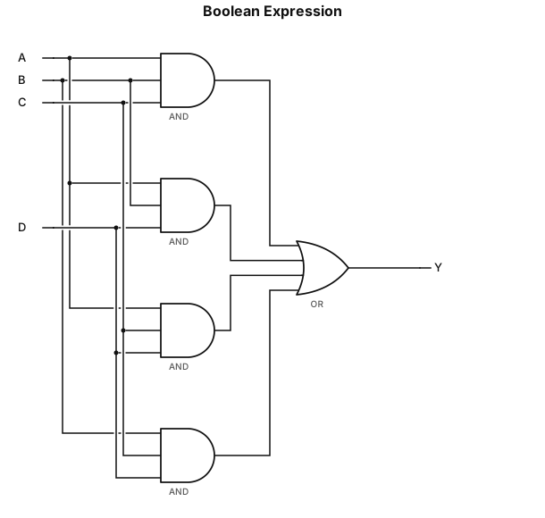
(ABC)+(ABD)+(ACD)+(BCD)
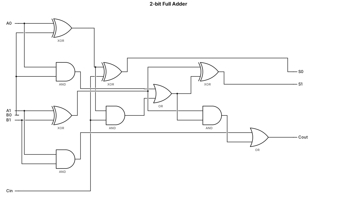
A logic gate circuit for a 2-bit full adder using AND, OR, and XOR gates with inputs A, B, and carry-in, and outputs sum and carry-out
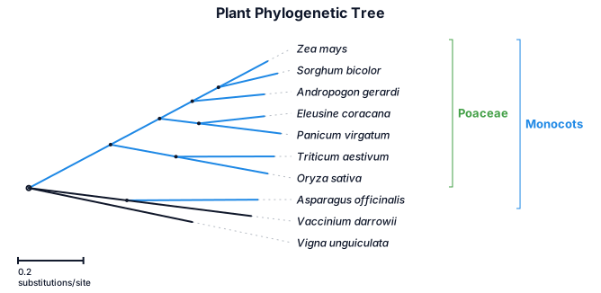
Vigna unguiculata Asparagus officinalis Triticum aestivum Zea mays Andropogon gerardi Sorghum bicolor Eleusine coracana Vaccinium darrowii Panicum virgatum Oryza Sativa
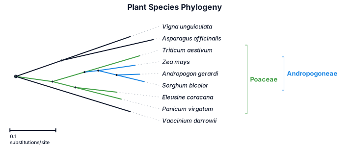
Vigna unguiculata Asparagus officinalis Triticum aestivum Zea mays Andropogon gerardi Sorghum bicolor Eleusine coracana Vaccinium darrowii Panicum virgatum

A timing diagram for an I2C read transaction: SCL clock, SDA with START condition, 0x30,Write bit, ACK bit, 0x03,ACK bit, 0x01, ACK bit and STOP condition

A timing diagram for an I2C read transaction: SCL clock, SDA with START condition, 0x30,Write bit, ACK bit, 0x01,ACK bit, 0x03, ACK bit and STOP condition
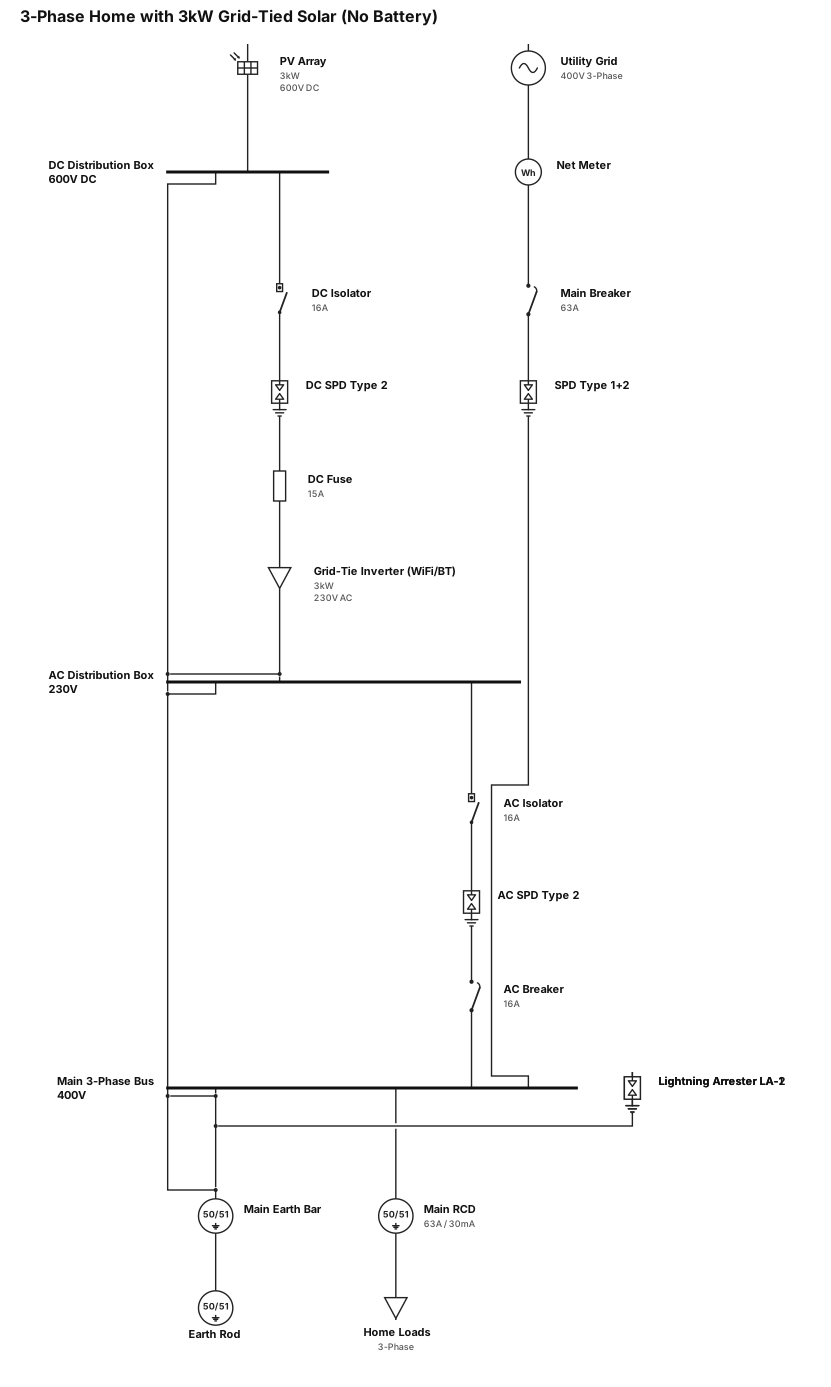
A single line diagram for a 3 phase home wiring but single phase solar installation without battery, on grid for 3kW, including DCDB, ACDB, invertor with wifi / bluetooth. Include LA and earthing considerations for the entire setup. use color codes compliant to solar residential for wires and other
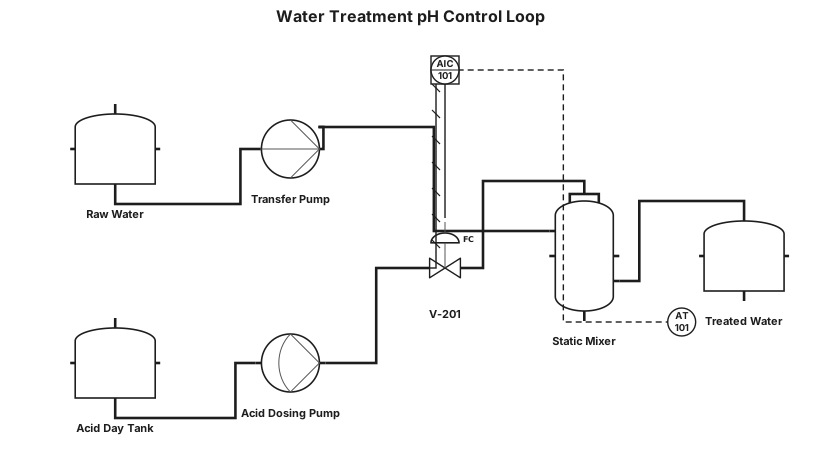
Water treatment loop with pH control and dosing pump