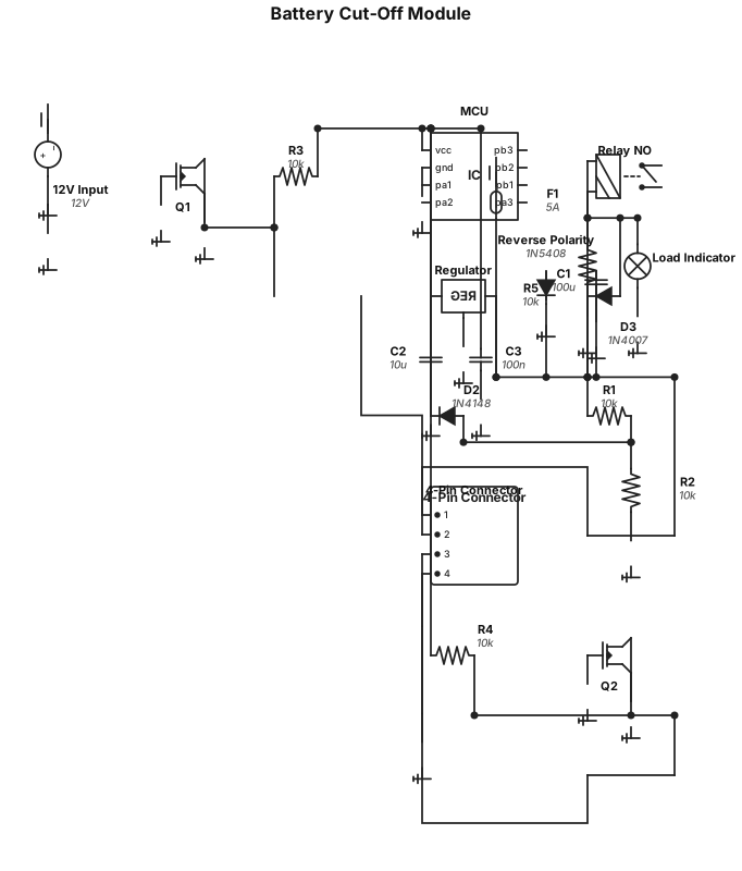
design battery cut off module circuit with 12v input, mcu, regulator, relay no, and 4 pin connector, active high pin 2 12v come from vehicle and active low 0v come from vehicle
NODE ARCHIVE · REAL DIAGRAM BRIEFS
Diagram Examples from Real Visitor Prompts
Browse eligible diagrams shared by FreeDiagram visitors, inspect the exact prompts, and build your own version.
Browse 1008 real creationsCOMMUNITY OUTPUTS · EXACT PROMPTS
Circuit Diagrams
Showing 25–48 of 49. No stock examples or system defaults. Choose a tool, study a real result, then reopen its prompt as your starting point.
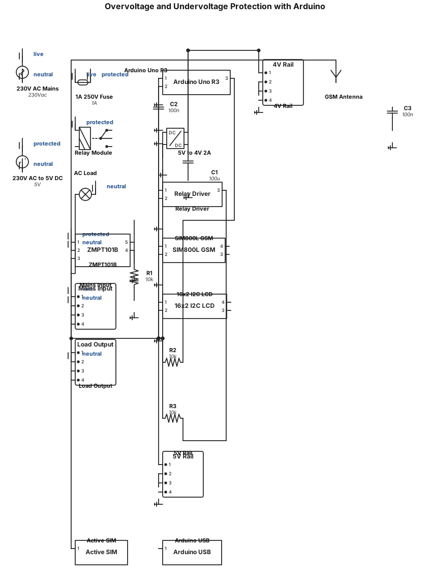
draw an overvoltage and undervoltage protection with these components are Arduino Uno R3, ZMPT101B AC voltage sensor module, 1-channel 5V relay module, SIM800L GSM module, 16×2 I²C LCD display, 230V AC to 5V DC regulated power supply, 5V DC to 4V DC 2A converter, 1A 250V AC fuse, 5×20mm fuse holder, full-size 830-point solderless breadboard, Dupont jumper wires, 230V AC mains input connector, AC appliance/load, AC outlet/load socket, SIM800L GSM antenna, active SIM card, and Arduino USB cable.
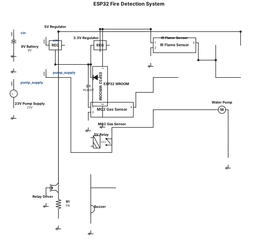
an esp 32 wroom where pump is connected to 5vdc relay to 9v battery and to pump to 23 then ir flame sensor is connected to esp through gpio4 and mq2 a0 is connected to esp through 34 and buzzer is connected to 18
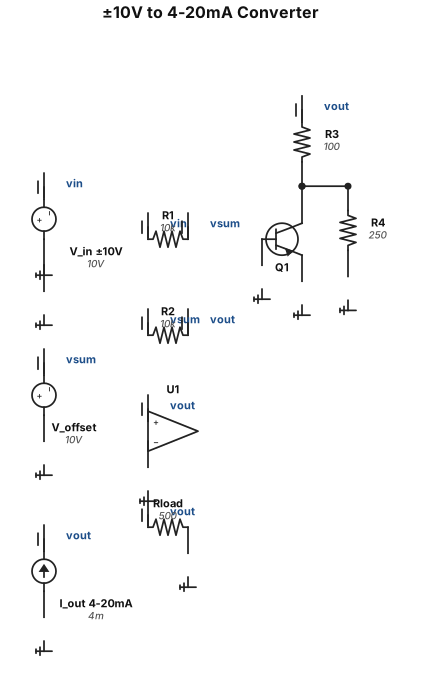
generate circuit for +/-10V as input and 4 to 20mA as output
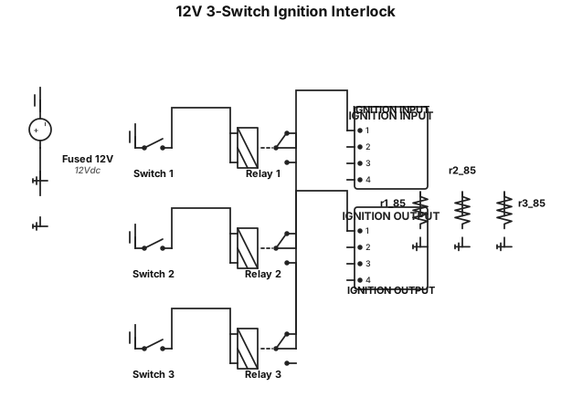
Create a simple 12V automotive 3-switch ignition interlock schematic. Use THREE Bosch-style 5-pin SPDT automotive relays. Clearly label EVERY relay terminal: 30, 85, 86, 87, and 87a. Each relay is controlled by one SPST toggle switch: * Terminal 85 of each relay goes to ground. * Terminal 86 receives fused 12V through its corresponding switch. The ONLY switch combination that should provide continuity from IGNITION INPUT to IGNITION OUTPUT is: Switch 1 = ON Switch 2 = OFF Switch 3 = ON Wire the ignition signal path exactly like this: IGNITION INPUT → Relay 1 terminal 30 Relay 1 terminal 87 → Relay 2 terminal 30 Relay 2 terminal 87a → Relay 3 terminal 30 Relay 3 terminal 87 → IGNITION OUTPUT Relay 1 must be energized for continuity. Relay 2 must be DE-ENERGIZED for continuity. Relay 3 must be energized for continuity. Do NOT add an ignition coil, ballast resistor, distributor, ECU, starter, battery charging system, or any other vehicle components. Do NOT invent additional connections. Show only: * Fused 12V control power * 3 toggle switches * 3 SPDT relays * Grounds * IGNITION INPUT * IGNITION OUTPUT Make the schematic suitable for physically wiring standard automotive relays and clearly show all terminal numbers.
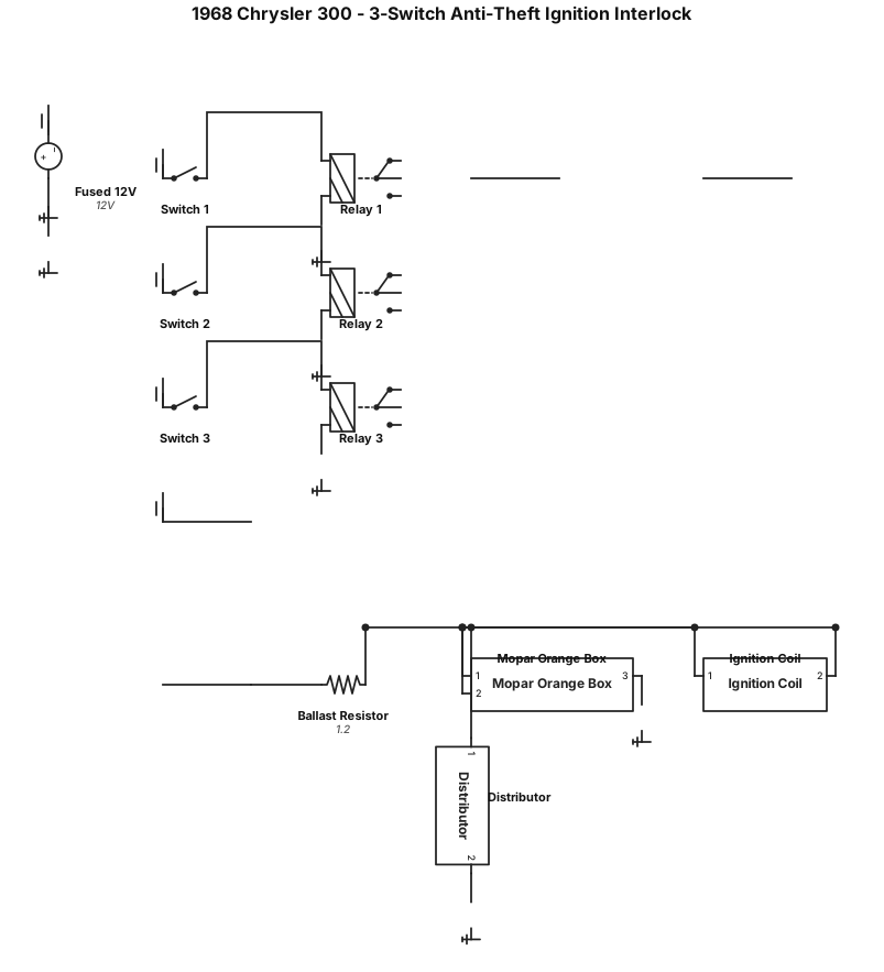
Create a 12V automotive wiring diagram for a 1968 Chrysler 300 with a 440 V8 and Mopar Orange Box electronic ignition. I want a 3-switch anti-theft ignition interlock using three 12V Bosch-style 5-pin SPDT relays (30, 85, 86, 87, 87a). The ignition should receive power ONLY with this combination: Switch 1 = ON Switch 2 = OFF Switch 3 = ON Each switch controls its relay coil: terminal 85 to ground and terminal 86 through its switch to fused 12V. Wire the ignition-enable path in series: Ignition source → Relay 1 terminal 30 → 87 → Relay 2 terminal 30 → 87a → Relay 3 terminal 30 → 87 → ignition system. Relay 1 uses 87 because Switch 1 must be ON. Relay 2 uses 87a because Switch 2 must be OFF. Relay 3 uses 87 because Switch 3 must be ON. Clearly label all relay terminals, switches, fused 12V, grounds, ignition input, and ignition output. Show the Mopar Orange Box, ballast resistor, ignition coil, and distributor for context. This circuit disables ignition/spark, not starter-motor power. Only ON-OFF-ON should allow the engine to have ignition.
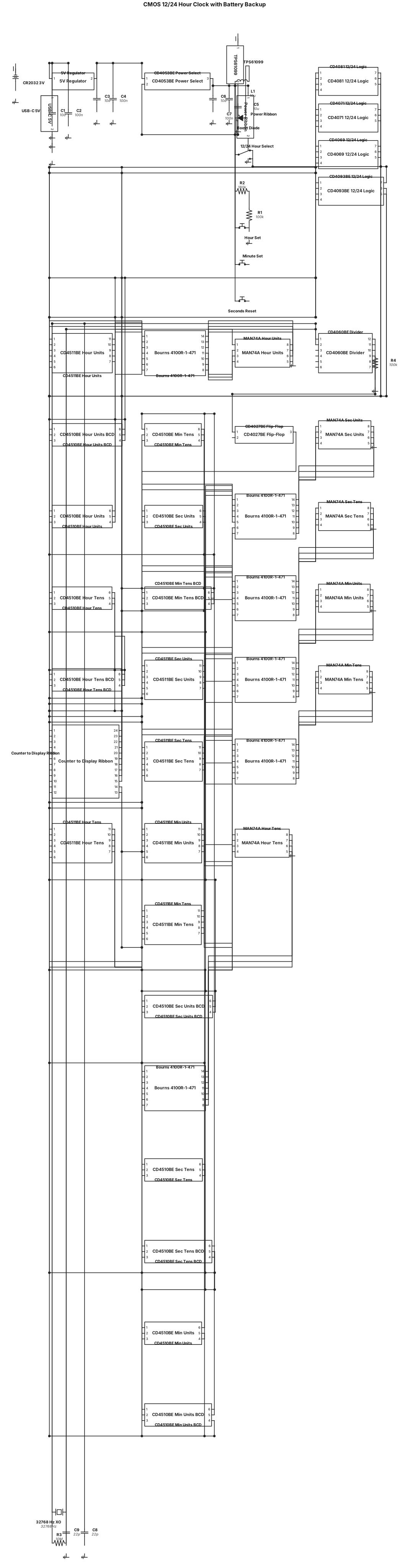
Using through-hole components where possible , create the following circuit, 12/24 hour clock using CMOS chips namely the cd4510be and the cd4511. Timebase will be a 32768 kHz Crystal Oscillator (XO), cd4060be and a cd4027be to get the 1Hz. Displays for the time will be MAN74A seven segment displays using 14 pin dip sockets current limit will be via six Bourns 4100R-1-471 isolated 470Ω resistor networks in a 14 pin dip package. The clock display will be HH:MM:SS Counter board should contain the timebase, 6 x cd4510 and any addition logic chips, display board should contain the MAN74A displays, 6x cd4511be and the six Bourns 4100R-1-471 isolated 470Ω resistor networks in a 14 pin dip package. Boards should be connected via ribbon connectors The power for the circuit will come from a USBC connector, for battery backup use the TPS61099, design for a 3 V CR2032 coin cell that powers only the oscillator/counters while automatically blanking the displays. Normal operation would use a regulated 5 V input. For time setting add hour-set, minute-set, seconds-reset pushbuttons, plus a 12/24-hour selector switch?. Do not use the ADA4927, need to keep the design all CMOS where ever possible try using the cd4053be instead and chips like the cd4093be, cd4081, cd4071, cd4069 for 12/24 hour logic.
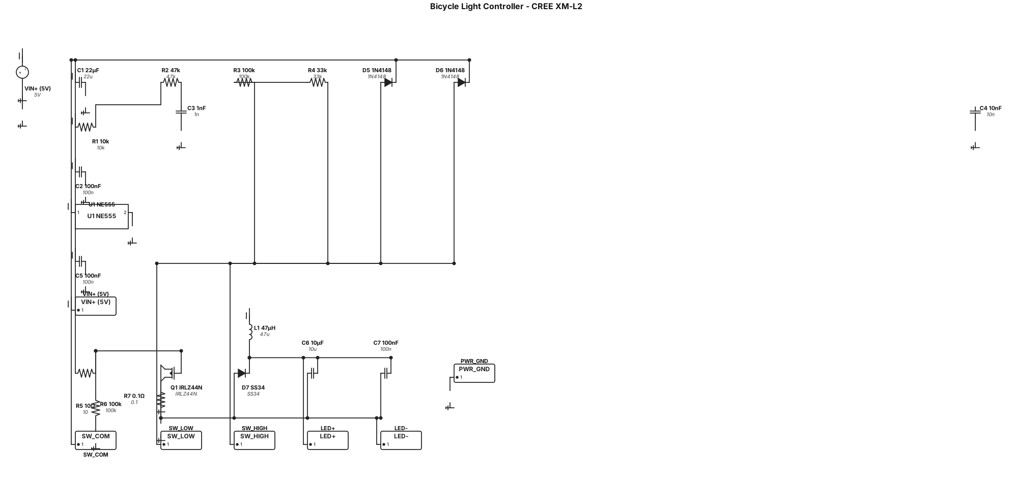
Create a bicycle light controller for a CREE XM-L2 LED - Fit on a 22mm O.D. circular printed circuit board. No through-hole solder pads. - the XM-L2 LED is on a separate board that will be connected by two wires that will be soldered to the controller pcb. - it will have an external spdt switch for low-off-high (on-off-on) operation with solder pads for the external SPDT switch wiring. Three solder pads for the external switch. Current requirements are average current with small deviation. Do not run led power through the switch. low power - 0.25 Amp average draw off high power - 2.00 Amp average draw - use high-frequency modulated operation to reduce power and heat - design for an external 5V battery supply that uses a YH11062B boost converter with a 27100 lithium cell. Solder pads for power need to be on the same side of the pcb as the switch solder pads. USe two solder pads for the input power. - solder pads for the XM-L2 led need to be on the opposite side of the pcb from the power and switch pads. - Modulate the XM-L2 led at high frequency to help limit heat generation and power consumption and to extend led lifetime. - produce schematic and pcb design layout for easyeda pro and kicad - Use pure hardware PWM without firmware - the 5V output from the YH11062B be assumed clean and regulated changes/notes from the offered design : - VIN+ next to PWR_GND - SW_GND isolated from LED return - Switch current isolated from LED current - LED pads opposite side - 2A current path widened - Driver thermal copper added - PWM hardware only - No firmware dependency
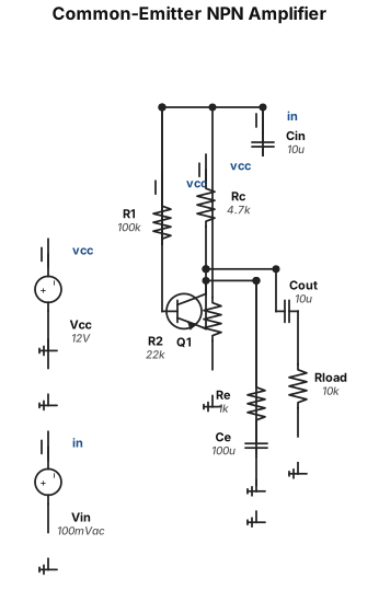
A common-emitter NPN transistor amplifier circuit
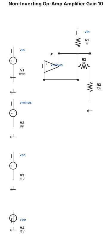
A non-inverting op-amp amplifier circuit with a gain of 10, using a 1 kΩ input resistor and a 9 kΩ feedback resistor complete circuit
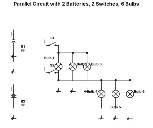
GENERATE A SCHEMATIC DIAGRAM IMAGE OF A PARALLEL CIRCUIT WITH 2 BATTERIES, 2 SWITCH, 6 BULBS
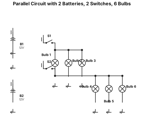
GENERATE A SCHEMATIC DIAGRAM IMAGE OF A PARALLEL CIRCUIT WITH 2 BATTERIES, 2 SWITCH, 6 BULBS, 25 WIRES
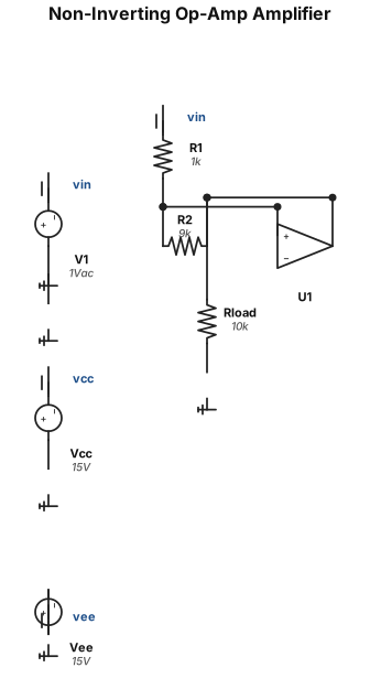
A non-inverting op-amp amplifier circuit with a gain of 10, using a 1 kΩ input resistor and a 9 kΩ feedback resistor
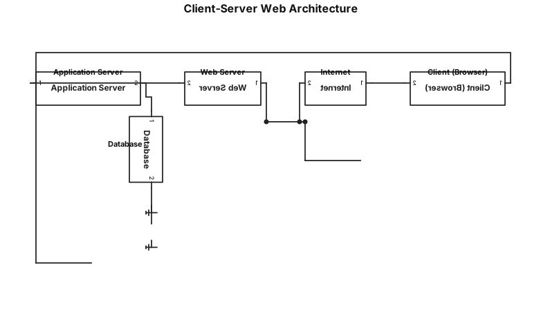
Общая схема клиент-серверного взаимодействия в веб. Клиент (браузер) — Интернет — Веб-сервер — Сервер приложений — База данных. Разделение на frontend и backend.
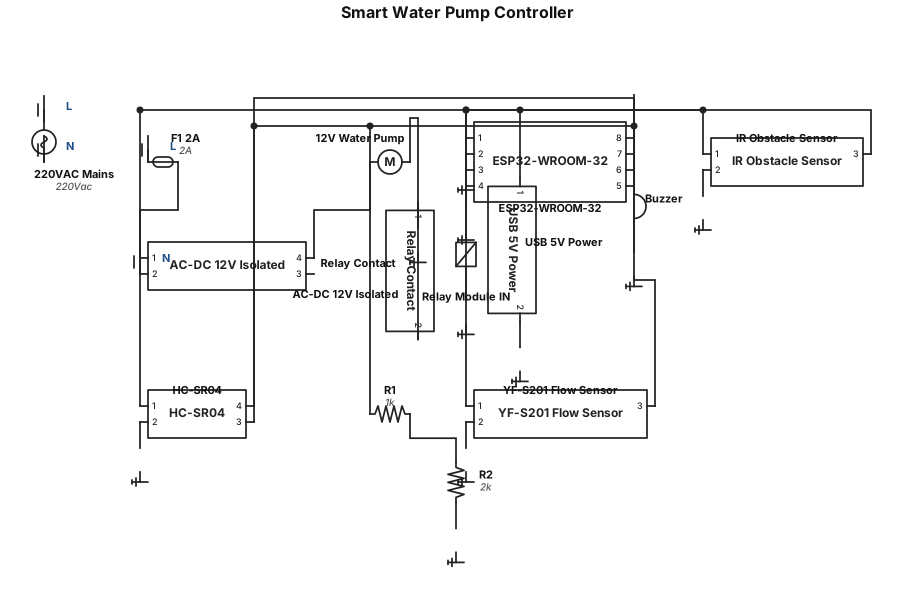
Create a professional electronics schematic for a smart water pump controller. Main controller: - ESP32-WROOM-32 development board powered by 5V USB. - Use common ESP32 DevKit pin labels. Connections: - IR obstacle sensor: VCC -> 5V GND -> GND OUT -> ESP32 GPIO32 - Relay module: VCC -> 5V GND -> GND IN -> ESP32 GPIO22 Relay contacts: COM connected to 12V pump supply line NO connected to pump positive terminal Pump negative connected to 12V power supply negative - Ultrasonic sensor HC-SR04: VCC -> 5V GND -> GND TRIG -> ESP32 GPIO5 ECHO -> ESP32 GPIO18 Add voltage divider on ECHO because ESP32 GPIO is 3.3V tolerant only. - Water flow sensor YF-S201: Red wire -> 5V Black wire -> GND Yellow wire -> ESP32 GPIO27 - Buzzer: Positive -> ESP32 GPIO19 Negative -> GND Power section: - Show separate 220VAC input. - 220VAC goes to an isolated AC-DC converter module producing 12V DC for the pump. - Show ESP32 5V USB power separately. - Keep AC mains section isolated from low voltage electronics. Draw as an engineering schematic, not a breadboard diagram. Use standard electrical symbols and labels.
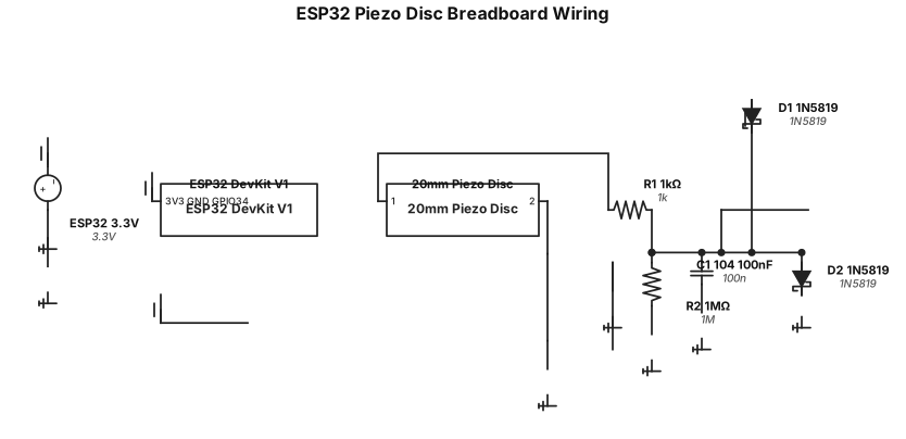
Create a clear beginner-friendly breadboard wiring diagram for testing ONE 20 mm piezoelectric disc with an ESP32 DevKit V1. Components: - ESP32 DevKit V1 - 20 mm piezo disc - R1 = 1 kΩ resistor - R2 = 1 MΩ resistor - C1 = 104 ceramic capacitor = 100 nF = 0.1 µF - D1 = 1N5819 Schottky diode - D2 = 1N5819 Schottky diode Use GPIO34 as the analog input. Connections: Piezo positive/ceramic side → R1 1 kΩ → sensing junction. Sensing junction → ESP32 GPIO34. Sensing junction → R2 1 MΩ → ESP32 GND. Sensing junction → C1 100 nF → ESP32 GND. For the positive clamp diode D1: D1 anode → sensing junction. D1 cathode (striped end) → ESP32 3.3 V. For the negative clamp diode D2: D2 anode → ESP32 GND. D2 cathode (striped end) → sensing junction. Piezo negative/brass side → ESP32 GND. Show EVERY wire separately. Show ESP32 3.3 V and GND clearly. Label the striped/cathode end of each 1N5819. Do not combine multiple connections into an unclear symbol. Use a breadboard-style wiring diagram, not only a schematic. Clearly label the sensing junction as "GPIO34 SENSING JUNCTION".
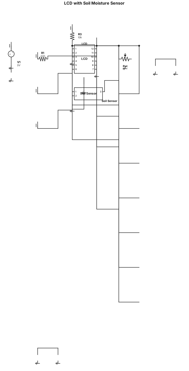
Create a circuit diagram with these exact connections: LCD: VSS → GND VDD → 5V VO → Potentiometer middle pin RS → D7 RW → GND E → D8 D4 → D9 D5 → D10 D6 → D11 D7 → D12 A/LED+ → 5V through 220Ω resistor K/LED− → GND Potentiometer: One end → GND Other end → 5V Middle pin → LCD VO Soil Moisture Sensor: VCC → 5V GND → GND SIG/AO → A0
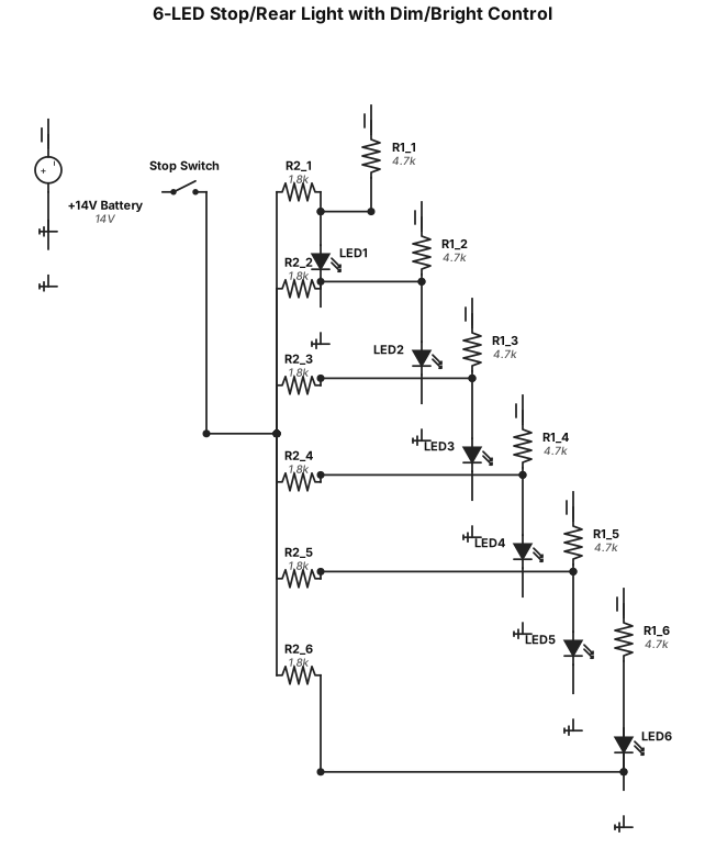
Create a clear electrical schematic for a 6-LED combined stop/rear light circuit. The six LEDs must be physically arranged in a 3-row × 2-column grid. Power supply: 12–14 V DC car battery. For each of the 6 LEDs, create one identical circuit branch. Each LED must have its own resistor network consisting of: R1 = 4.7 kΩ R2 = 1.8 kΩ R1 and R2 must be connected in parallel with each other, and this parallel resistor combination must be in series with its LED. Use exactly ONE SPST switch. The switch must simultaneously control all six R2 = 1.8 kΩ branches. When the switch is OPEN: only the 4.7 kΩ resistor is active for each LED, producing the dim rear-position mode. When the switch is CLOSED: the 1.8 kΩ resistor is added in parallel with the 4.7 kΩ resistor for each LED, producing the bright stop mode. All six LED branches must be connected across the battery in parallel so that each LED has its own identical resistor network and receives equal current. Use standard electrical schematic symbols. Clearly label: +14 V battery, GND, all six LEDs, all six 4.7 kΩ resistors, all six 1.8 kΩ resistors, and the single SPST switch. Do not connect the six LEDs in series. Do not use six switches. Make the circuit topology equivalent to the single-LED circuit shown in Figure 4, replicated six times with one common switch.
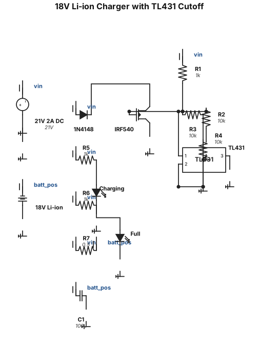
Hey I have Dewalt 18v 2.0 AH li-on battery now I am charging this battery with 21v 2A dc power supply now I need two indicators one for battery charging and other one for when battery full charged led need to glow and also need cut off circuit after full charge circuit need turn off automatically using TL431 full connection in easy way beginners can understand
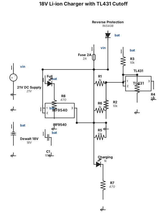
Hey I have Dewalt 18v 2.0 AH li-on battery now I am charging this battery with 21v 2A dc power supply now I need two indicators one for battery charging and other one for when battery full charged led need to glow and also need cut off circuit after full charge circuit need turn off automatically using Tl431

Create a complete, buildable schematic for a MONO 2-band Baxandall audio tone control preamplifier. POWER: - Single +12V DC supply - GND = 0V - Create VREF = +6V using two 10kΩ resistors as a voltage divider. - Add 100µF and 100nF capacitors from VREF to GND. - Use NE5532 dual op-amp. - Show the correct NE5532 pin numbers and power pins. - NE5532 pin 8 = +12V - NE5532 pin 4 = GND AUDIO INPUT: - Mono audio input - Input coupling capacitor = 1µF - Input bias/reference must be connected correctly to VREF. - Add an input volume control using a 50kΩ potentiometer. TONE CONTROL: - Use a proper ACTIVE Baxandall 2-band tone control. - Bass control = 50kΩ potentiometer. - Treble control = 50kΩ potentiometer. - Bass center frequency approximately 100Hz. - Treble center frequency approximately 10kHz. - Tone controls must be centered around VREF for single-supply operation. - Clearly show every resistor and capacitor value. - Clearly show every connection between the tone-control components and the NE5532. OUTPUT: - Mono audio output. - Output must be biased correctly around VREF. - Add an output coupling capacitor so the external amplifier receives no DC. - Output should be suitable for a TPA3116D2 Class-D amplifier input. IMPORTANT: - Use standard electronic schematic symbols. - Show ALL component values. - Show ALL NE5532 pin numbers. - Show +12V, GND and VREF clearly. - Do not omit any component. - Do not use a generic block diagram. - Generate a real electronic schematic with wires and component symbols. - Make it clean, large and easy to read. - The final result must be suitable for manually rebuilding on a PCB.
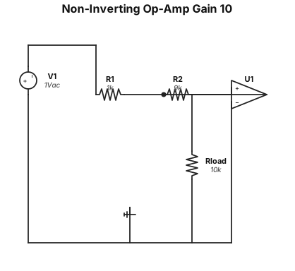
A non-inverting op-amp amplifier circuit with a gain of 10, using a 1 kΩ input resistor and a 9 kΩ feedback resistor
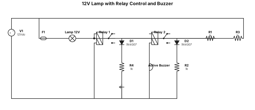
Нарисуй простую электрическую схему: лампа 12 В стоит в силовой цепи вместо предохранителя. Лампа коммутируется нормально разомкнутым контактом реле 1. Катушка реле 1 включена параллельно силовой линии. Второе реле (реле 2) с перекидными контактами управляет активным зуммером: зуммер включён через нормально замкнутый контакт реле 2. Катушка реле 2 питается через NO‑контакт реле 1 (то есть при срабатывании реле 1 реле 2 тоже срабатывает и отключает зуммер). Добавь два защитных диода параллельно катушкам обоих реле. Используй стандартные символы компонентов и подпиши их.»
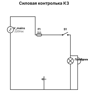
Нужна силовая контролька КЗ есть — лампа горит, зуммер молчит; КЗ нет — лампа не горит (или горит слабо), зуммер пищит.
Focused examples and prompt ideas
Start with the complete visitor wall above, then use these focused collections when you want a narrower subject and more prompt context.
The first curated collection is being prepared.