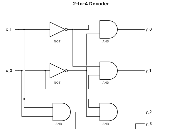
Task: Draw a circuit diagram of a 2-to-4 decoder based on a network of logic gates. Operation and logic: Inputs: x_1 and x_0 (a 2-bit binary number). Outputs: y_3, y_2, y_1, y_0 (one-hot encoding). Boolean equations: y_0 = \bar{x}_1 \bar{x}_0, y_1 = \bar{x}_1 x_0, y_2 = x_1 \bar{x}_0, y_3 = x_1 x_0. Diagram construction instructions: Place two input lines, x_1 and x_0, on the left side. Add NOT gates (inverters) to the input lines to obtain the negated signals \bar{x}_1 and \bar{x}_0. On the right side, place four 2-input AND gates (or AND gates with inverted inputs—indicated by "bubbles"). Connect the inputs to the AND gates as follows: First AND gate: inputs \bar{x}_1 and \bar{x}_0 \rightarrow output y_0. Second AND gate: inputs \bar{x}_1 and x_0 \rightarrow output y_1. Third AND gate: inputs x_1 and \bar{x}_0 \rightarrow output y_2. Fourth AND gate: inputs x_1 and x_0 \rightarrow output y_3. Label the inputs of all gates and... outputs clearly labeled (x_1, x_0, y_0, y_1, y_2, y_3). Draw the diagram with a clear white background and black lines. and can you make the x stand sidebyside and the y stand sidebyside
Diagram Examples from Real Visitor Prompts
Browse eligible diagrams shared by FreeDiagram visitors, inspect the exact prompts, and build your own version.
Browse 3265 real creationsAll visitor creations
Showing 265–288 of 3265. No stock examples or system defaults. Choose a tool, study a real result, then reopen its prompt as your starting point.
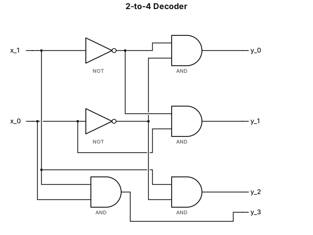
Task: Draw a circuit diagram of a 2-to-4 decoder based on a network of logic gates. Operation and logic: Inputs: x_1 and x_0 (a 2-bit binary number). Outputs: y_3, y_2, y_1, y_0 (one-hot encoding). Boolean equations: y_0 = \bar{x}_1 \bar{x}_0, y_1 = \bar{x}_1 x_0, y_2 = x_1 \bar{x}_0, y_3 = x_1 x_0. Diagram construction instructions: Place two input lines, x_1 and x_0, on the left side. Add NOT gates (inverters) to the input lines to obtain the negated signals \bar{x}_1 and \bar{x}_0. On the right side, place four 2-input AND gates (or AND gates with inverted inputs—indicated by "bubbles"). Connect the inputs to the AND gates as follows: First AND gate: inputs \bar{x}_1 and \bar{x}_0 \rightarrow output y_0. Second AND gate: inputs \bar{x}_1 and x_0 \rightarrow output y_1. Third AND gate: inputs x_1 and \bar{x}_0 \rightarrow output y_2. Fourth AND gate: inputs x_1 and x_0 \rightarrow output y_3. Label the inputs of all gates and... outputs clearly labeled (x_1, x_0, y_0, y_1, y_2, y_3). Draw the diagram with a clear white background and black lines.
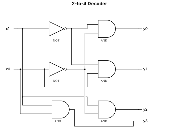
Task: Draw a circuit diagram of a 2-to-4 decoder based on a network of logic gates. Operation and logic: Inputs: $x_1$ and $x_0$ (a 2-bit binary number). Outputs: $y_3, y_2, y_1, y_0$ (one-hot encoding). Boolean equations: $y_0 = \bar{x}_1 \bar{x}_0$, $y_1 = \bar{x}_1 x_0$, $y_2 = x_1 \bar{x}_0$, $y_3 = x_1 x_0$. Diagram construction instructions: Place two input lines, $x_1$ and $x_0$, on the left side. Add NOT gates (inverters) to the input lines to obtain the negated signals $\bar{x}_1$ and $\bar{x}_0$. On the right side, place four 2-input AND gates (or AND gates with inverted inputs—indicated by "bubbles"). Connect the inputs to the AND gates as follows: First AND gate: inputs $\bar{x}_1$ and $\bar{x}_0 \rightarrow$ output $y_0$. Second AND gate: inputs $\bar{x}_1$ and $x_0 \rightarrow$ output $y_1$. Third AND gate: inputs $x_1$ and $\bar{x}_0 \rightarrow$ output $y_2$. Fourth AND gate: inputs $x_1$ and $x_0 \rightarrow$ output $y_3$. Label the inputs of all gates and... outputs clearly labeled ($x_1, x_0, y_0, y_1, y_2, y_3$). Draw the diagram with a clear white background and black lines.
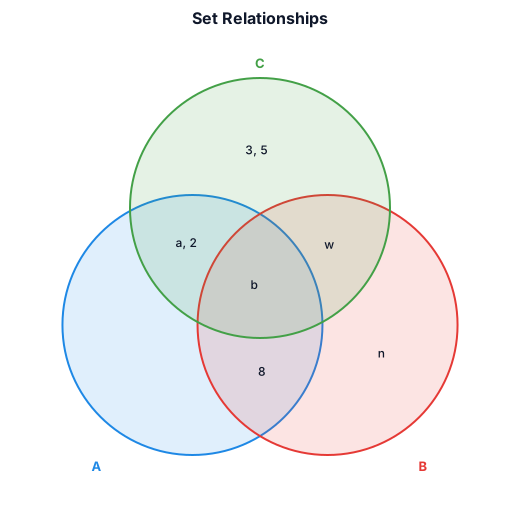
A={a,b,8,2} b={w,n,8,b} c={a,2,3,5,w,b}
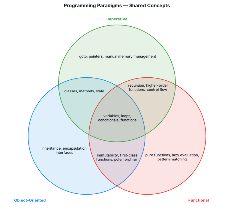
A three-set Venn diagram comparing object-oriented, functional, and imperative programming — show shared concepts like variables and loops in the overlapping regions

Create a professional high-level architecture diagram titled “High-Level Design of CSLM-IDE” for a B.Tech CSE project report. Use a white background, landscape layout, blue-accented rectangular blocks, readable black text and directional arrows. Organize the system into layers: 1. User Layer: Developer. 2. Presentation Layer: Title Bar, Activity Bar, Explorer, Monaco Code Editor, AI Assistant Panel, Terminal and Output, Status Bar, Settings. 3. Application Logic Layer: Workspace Management, Editor State, File Operations, Search, Keyboard Shortcuts, Conversion Request Coordinator. 4. Core Services Layer: AI Code Conversion Module, Language and Prompt Configuration, Validation and Error Feedback. 5. External Systems: Local File System, Gemini AI Model API, Installed Language Runtimes and Compilers. Connect the layers logically. Show filesystem access, AI request/response, and run/build interactions. Label this as a high-level design, not proof that every feature is implemented. No 3D effects, no decorative illustrations, no overlapping arrows. Keep every label legible.
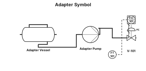
adapter
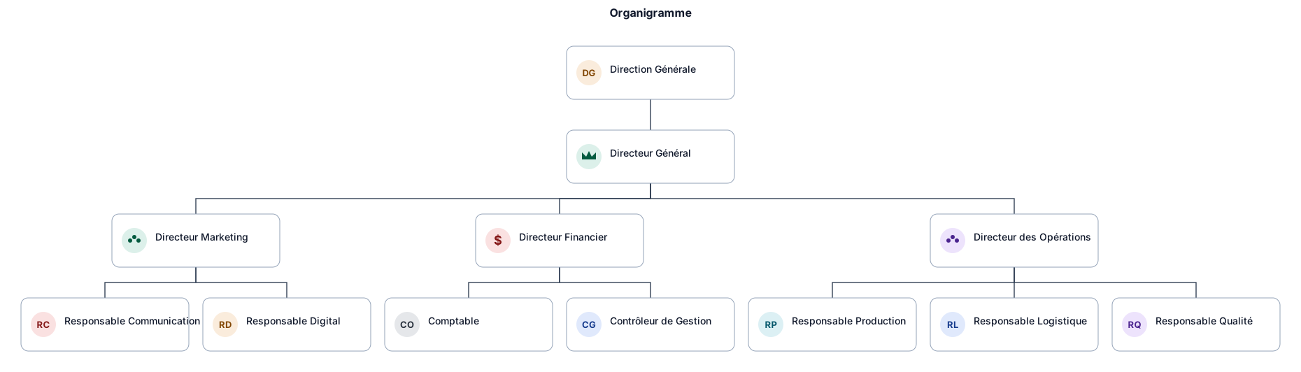
un organisgramme pour ma synthèse
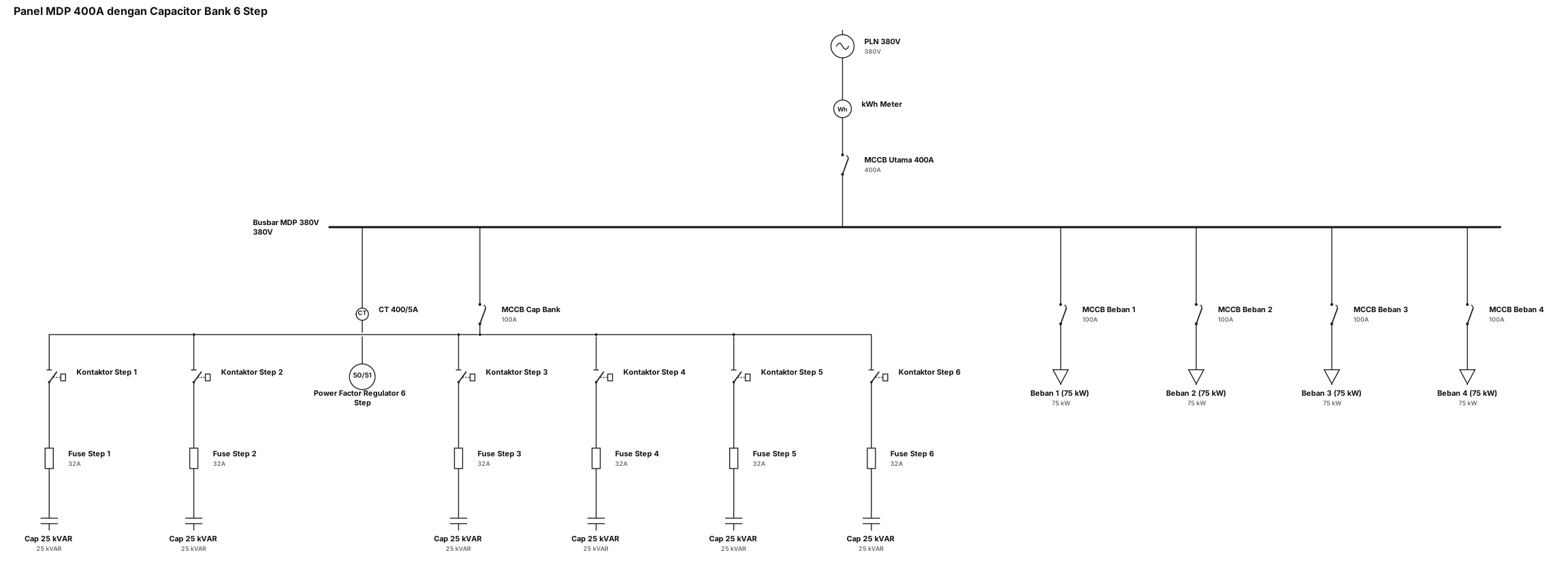
buatkan single line diagram panel mdp kapasitas 400 A dengan capasitor bank 6 step dengan beban daya 300 Kw sertakan equipment dalam panel
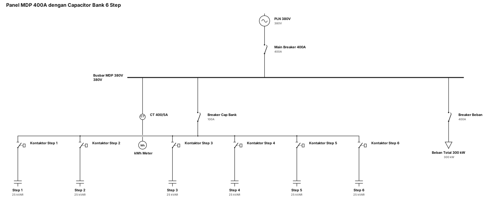
buatkan single line diagram panel mdp kapasitas 400 A dengan capasitor bank 6 step dengan beban daya 300 Kw
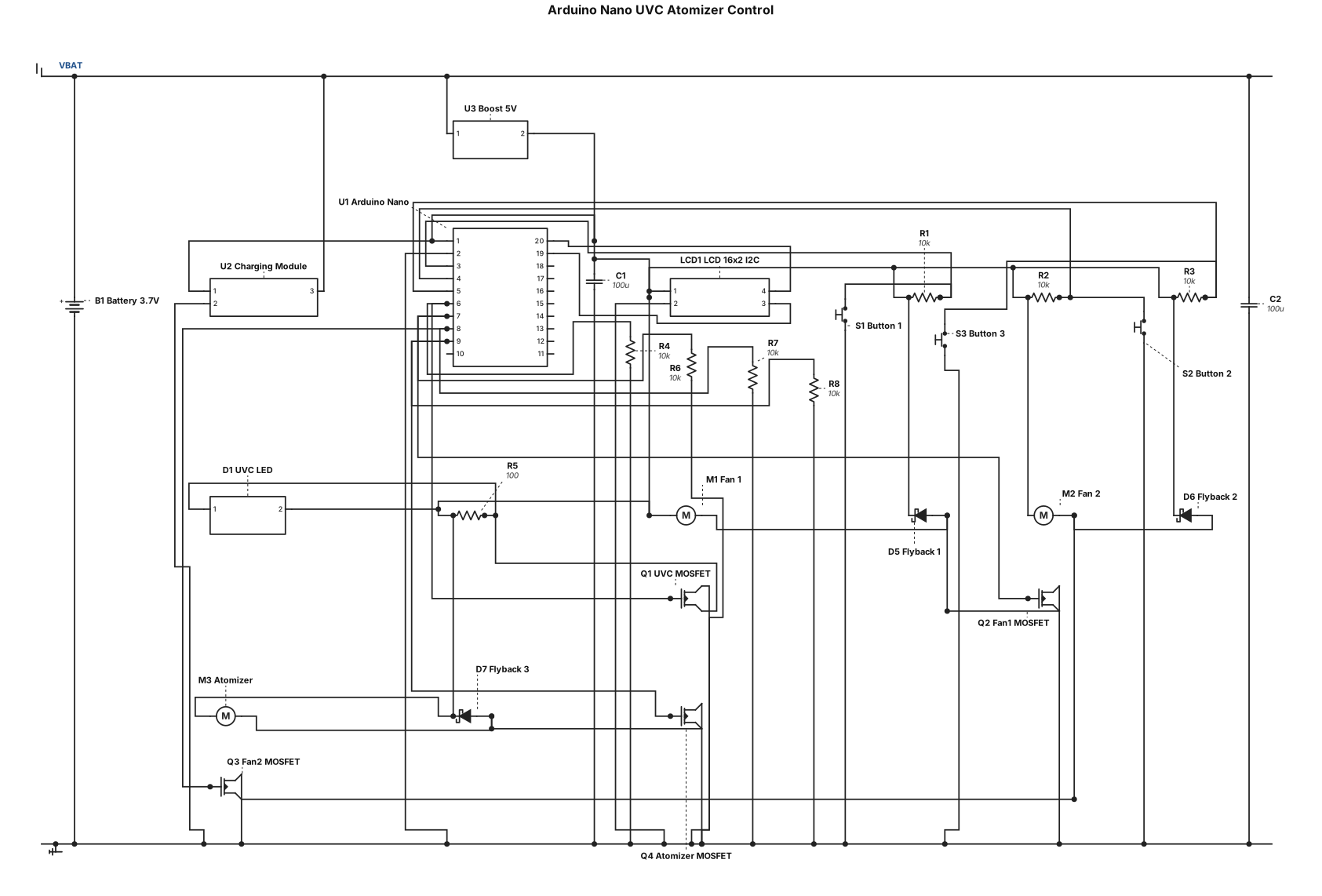
I want to create something that includes 1. Arduino Nano 2. 170 pin breadboard 3. LCD module 4. 3 Button Modules 5. UVC LED light 6. 3010 fans x 2 7. Atomizer 8. Charging port module 9. battery. Provide a circuit diagram for me
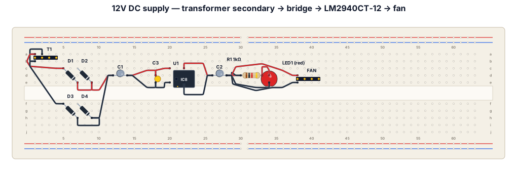
Create a clear, labeled breadboard wiring diagram for a 12V DC power supply to run an Intel PC fan rated at 12V DC, 600mA. The circuit must have these stages in order: 1. Transformer secondary: isolated 12V AC output, using only the two low-voltage secondary wires. Label the AC inputs AC1 and AC2. 2. Full-wave bridge rectifier using four individual 1N5408 diodes arranged in a diamond configuration. Label the positive DC output RAW+ and the negative output GND. Clearly show each diode's band and correct orientation. 3. Main filter capacitor C1: 6800uF, 35V electrolytic capacitor, with positive connected to RAW+ and negative connected to GND. 4. Fixed 12V regulator U1: LM2940CT-12 in a TO-220 package. Label the input, ground, output, and ground-connected metal tab correctly using the manufacturer's datasheet. 5. Input bypass capacitor: 0.47uF between regulator input and GND. 6. Output capacitor C2: 22uF electrolytic capacitor, connected between regulated +12V and GND. Show correct polarity and note that its ESR must meet the LM2940CT-12 datasheet requirements. 7. Power indicator: one red LED in series with a 1k ohm, 1/4W resistor across the regulated output, with correct polarity. 8. Output load: a 12V DC PC fan rated at 600mA, connected between +12V OUT and GND. Clearly label all nodes, component values, diode bands, capacitor polarity, regulator pins, and the positive and negative fan connections. Show the circuit stages from left to right in the order transformer secondary, bridge rectifier, filter capacitor, voltage regulator, and fan output. IMPORTANT: Show only the isolated low-voltage circuit. Do not include or expose 220V AC mains wiring on the breadboard. Do not invent connections if the software cannot represent a component correctly. Indicate that the finished circuit must be checked against the component datasheets and tested under supervision before connecting the fan.
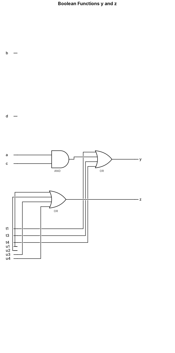
y = a'c' + ac + ab'd + bcd'; z = a'b'd + ab'd + bc'd' + bcd';
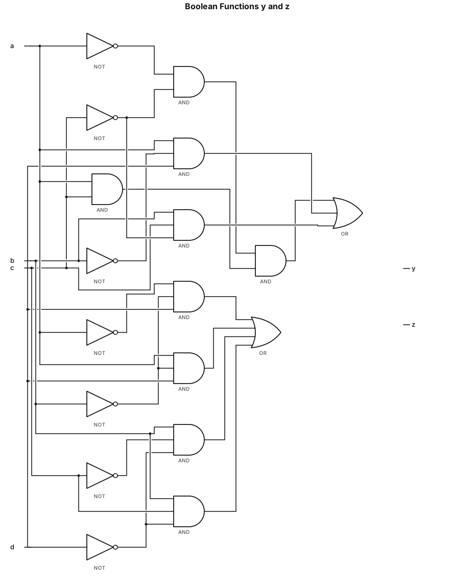
y = a'c' + ac + ab'd + bcd'; z = a'b'd + ab'd + bc'd' + bcd'
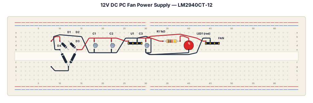
Create a breadboard wiring diagram for a 12V DC, 600mA PC fan power supply using these components: an isolated 12V AC transformer secondary, four 1N5408 diodes in a full-wave bridge rectifier, a 6800uF 35V electrolytic filter capacitor, an LM2940CT-12 fixed 12V voltage regulator, a 0.47uF input capacitor, a 22uF output capacitor with the required ESR, a red LED, and a 1k ohm 1/4W resistor. Connect the two 12V AC secondary wires to the two AC inputs of the four-diode bridge. Connect the bridge's positive output to RAW+ and its negative output to GND. Connect the 6800uF capacitor positive lead to RAW+ and negative lead to GND. Connect the LM2940CT-12 input pin to RAW+, its ground pin to GND, and its output pin to +12V OUT. Connect the 0.47uF input capacitor between regulator input and GND, and the 22uF output capacitor between +12V OUT and GND, respecting polarity and the regulator datasheet's ESR requirements. Connect the red LED and 1k ohm resistor in series across +12V OUT and GND. Connect the PC fan positive wire to +12V OUT and its negative wire to GND. Label every component, value, connection, diode band, capacitor polarity, and regulator pin. Show the four diodes as a diamond-shaped bridge rectifier. This circuit has no microcontroller. Show only the isolated low-voltage side, not the 220V AC mains wiring.
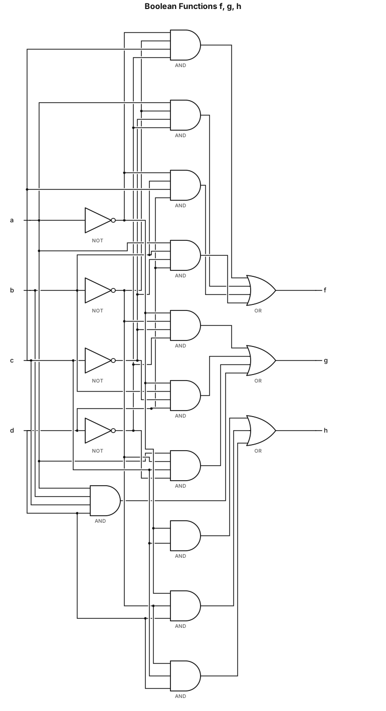
f = a'b'cd' + ab'c'd' + a'bcd + abc'd; a'b'c'd' + a'bc'd + ab'cd' + abcd; h = a'c + a'b'd + b'cd

a pump connected to a 6" pipe. Off of that pipe are 8 connections via T's, with an isolation valve at the connection point, and then a 4" line coming off of it with a sanitary connection at the end. At the end of the header loop back to the inlet of the pump

a pump connected to a 6" pipe. Off of that pipe are 8 connections via T's, with an isolation valve at the connection point, and then a 4" line coming off of it with a sanitary connection at the end

a pump connected to a 4" pipe. Off of that pipe are 8 connections via T's, with an isolation valve at the connection point, and then a 4" line coming off of it with a sanitary connection at the end
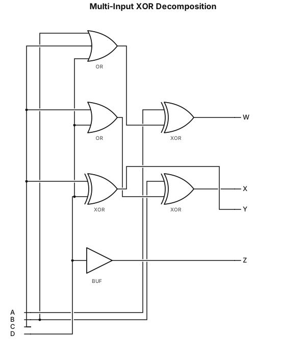
W=A⊕(B+C+D);X=B⊕(C+D);Y=C⊕D;Z=D plot using two input gates
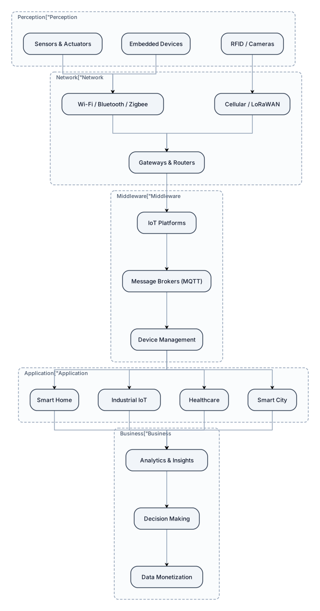
A flowchart explaining Internet of things(IoT) architecture
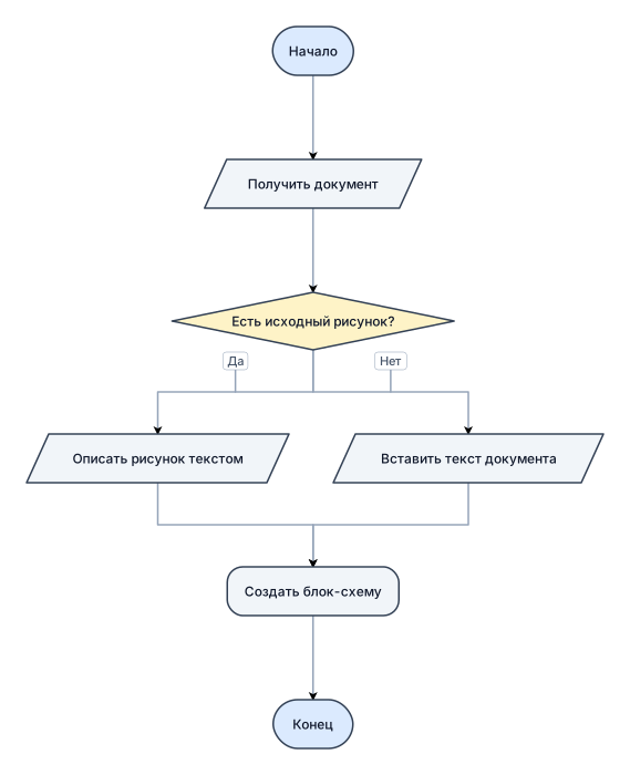
привет , мне нужно сделать блок схему к документу. что тебе нужно для этого я могу предоставить исходный рисунок над которым можно дальше работать
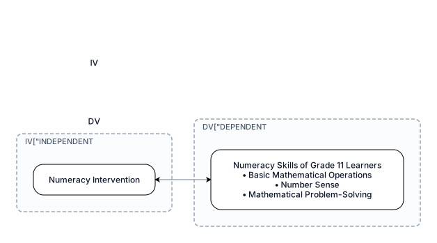
Create a clean, professional, academic research paradigm for a quantitative correlational study entitled “Relationship Between Numeracy Intervention and Numeracy Skills of Grade 11 Learners.” Use the Independent Variable–Dependent Variable framework, NOT the IPO model. Layout: 1. On the left, create a rectangular box labeled “INDEPENDENT VARIABLE.” Inside, write “Numeracy Intervention.” 2. On the right, create a rectangular box labeled “DEPENDENT VARIABLE.” Inside, write “Numeracy Skills of Grade 11 Learners,” with these indicators: Basic Mathematical Operations; Number Sense; Mathematical Problem-Solving. 3. Connect the two boxes with a horizontal, double-headed arrow to represent the relationship being investigated between the variables. Do not imply cause and effect. Design requirements: simple formal academic style, white background, black text, thin black borders, equal-sized horizontally aligned boxes, readable serif font similar to Times New Roman, correct spelling, landscape page, no unnecessary icons or decorations, suitable for Chapter 1 of a senior high school research paper. Add this caption below the diagram: “Figure 1. Research Paradigm Illustrating the Relationship Between Numeracy Intervention and Numeracy Skills of Grade 11 Learners.” Ensure the diagram is appropriate for a correlational study and contains only the specified variables and indicators.
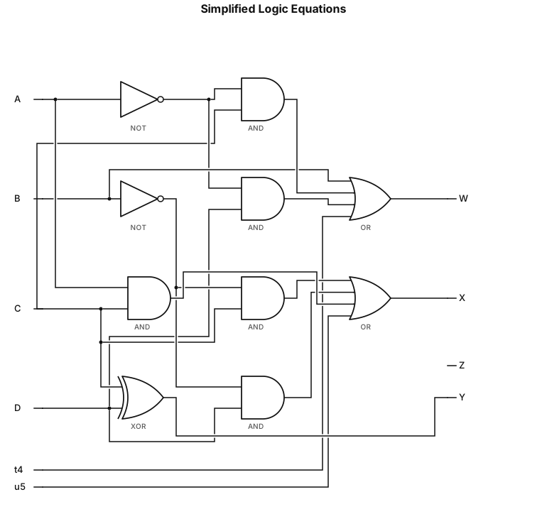
Final Simplified Equations Summary • \(\mathbf{W=B+A}^{\prime }\mathbf{C+A}^{\prime }\mathbf{D+AD}^{\prime }\) • \(\mathbf{X=B}^{\prime }\mathbf{C+B}^{\prime }\mathbf{D+AC+BC}^{\prime }\mathbf{D}^{\prime }\) • \(\mathbf{Y=C\oplus D}\) • \(\mathbf{Z=D}\)