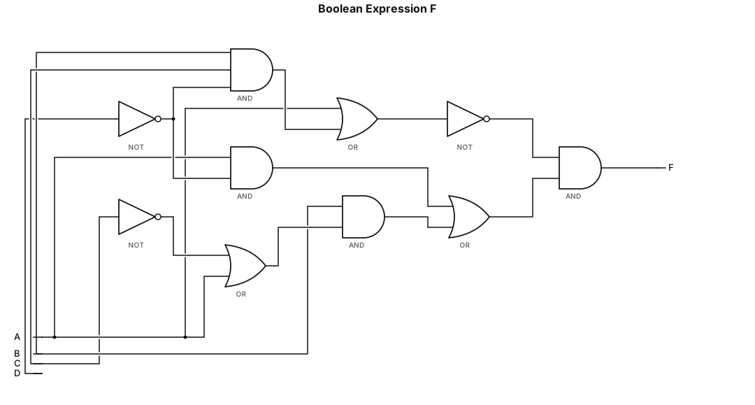
b) F = [A + BCD ̅̅̅̅̅̅ ][AD̅̅̅̅ + B(C̅ + A)]
NODE ARCHIVE · REAL DIAGRAM BRIEFS
Diagram Examples from Real Visitor Prompts
Browse eligible diagrams shared by FreeDiagram visitors, inspect the exact prompts, and build your own version.
Browse 3276 real creationsCOMMUNITY OUTPUTS · EXACT PROMPTS
All visitor creations
Showing 481–504 of 3276. No stock examples or system defaults. Choose a tool, study a real result, then reopen its prompt as your starting point.
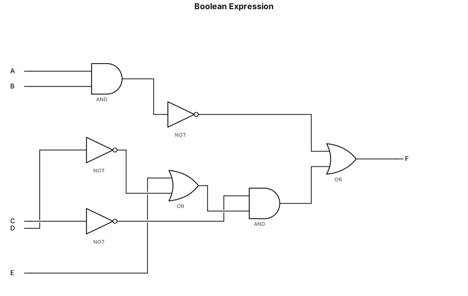
F = (AB)'+ C̅(E + D̅)
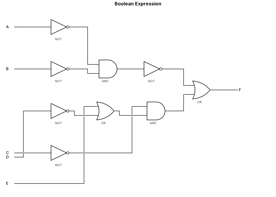
F = A'B̅̅̅̅ + C̅(E + D̅)
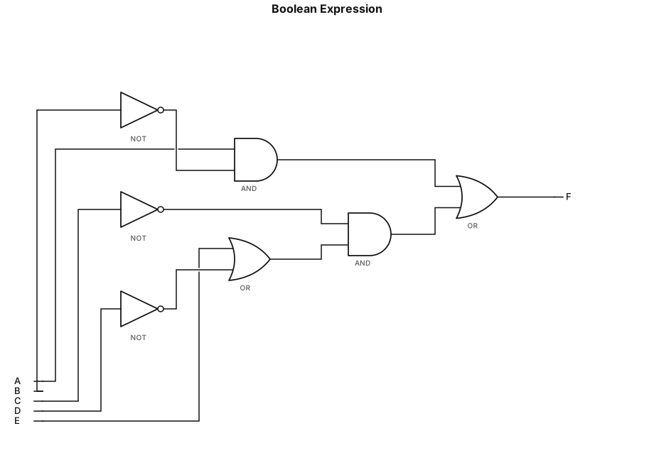
F = AB̅̅̅̅ + C̅(E + D̅)
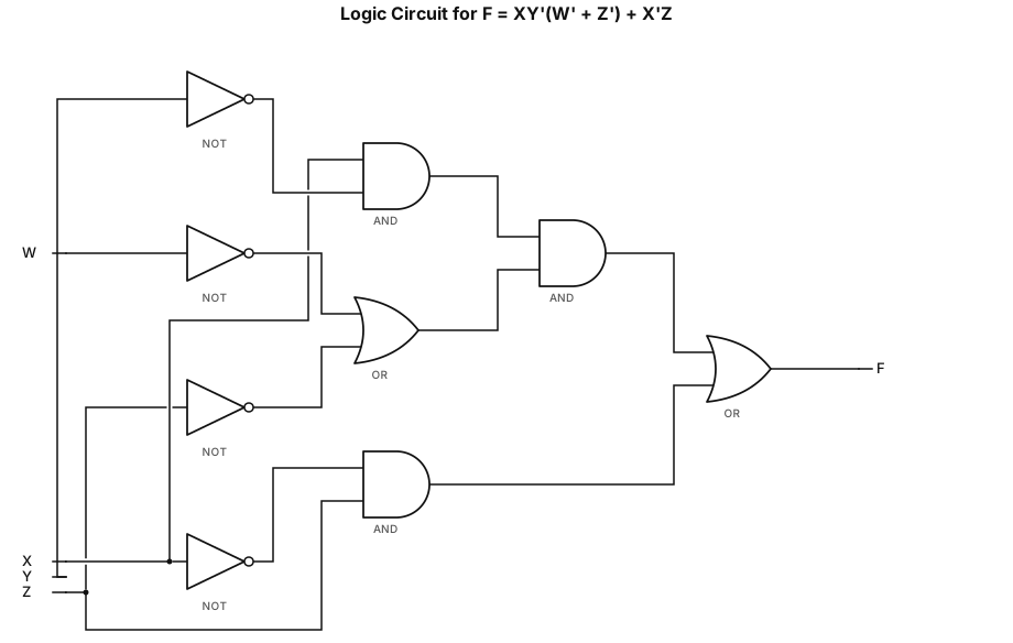
Draw the logic circuit diagram for F = XY'(W' + Z') + X'Z, strictly using NOT gates and two-input AND/OR gates. Inputs W, X, Y, Z; output F.
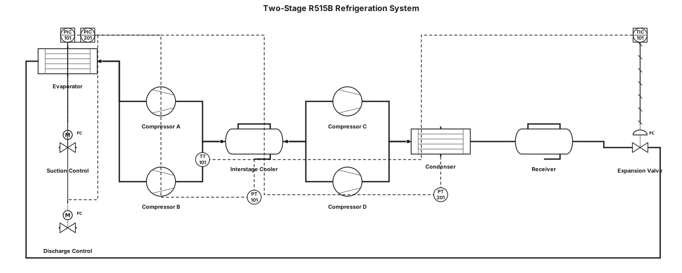
two stage refrigeration system for R515B with tandem scroll compressors and inter stage cooler vessel
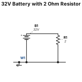
32v battery in series with 2 ohm resistor
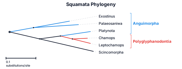
exostinus, palaeosaniwa, platynota, chamops, leptochamops, scincomorpha
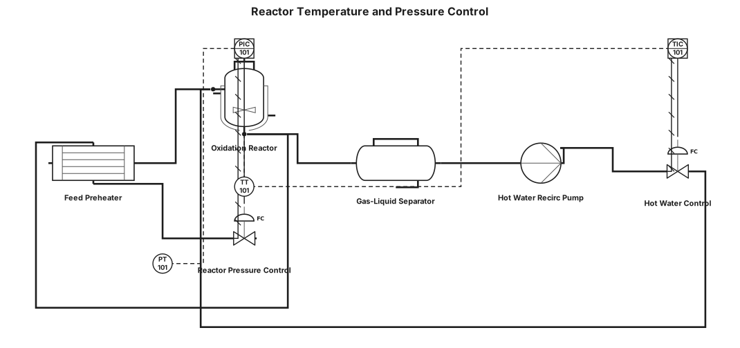
Feed gas is preheated in FP-01 using heat recovered from reactor effluent before entering reactor R-101. The oxidation reaction is highly exothermic, and heat is removed by circulating hot water through the shell side of the reactor. The heated water is separated into GLS-1 and recirculated by P-01. Reactor pressure is controlled through the effluent-side pressure control valve while reactor temperature is controlled through hot water circulation.
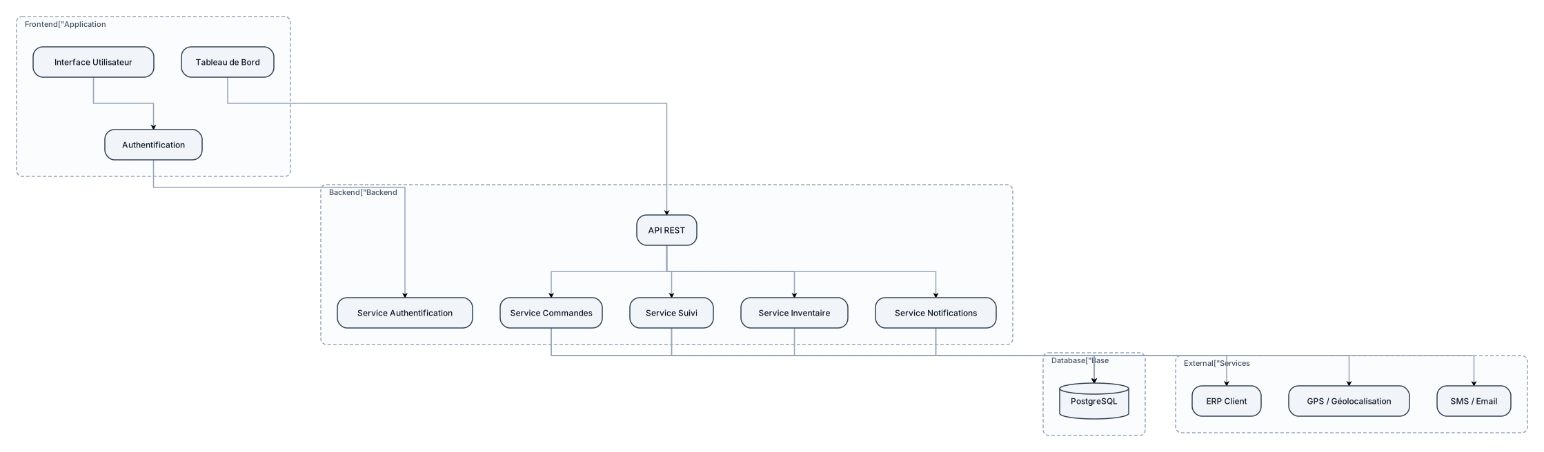
CREAT UN DIGRAME POUR UN APPLICATION SUIVI LOGISTIQUE
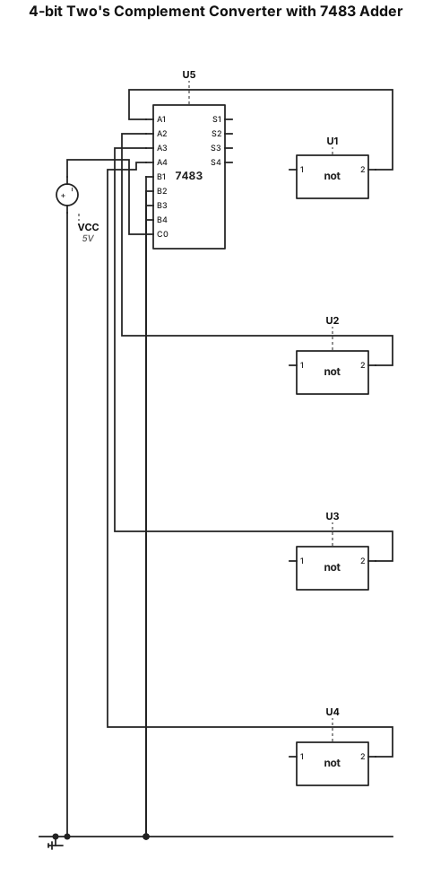
Create a detailed schematic of a 4-bit Two's Complement converter with a 7483 4-bit adder chip: Inputs A0, A1, A2, A3 pass through four NOT gates to invert all bits. The outputs of the NOT gates connect to inputs A1, A2, A3, A4 of the 7483 adder. Inputs B1, B2, B3, B4 of the 7483 are tied to GND (0). Carry-in (C0 or Cin) is tied to VCC (1) to add the +1 required for Two's Complement. Outputs S1, S2, S3, S4 show the final 4-bit Two's Complement result.
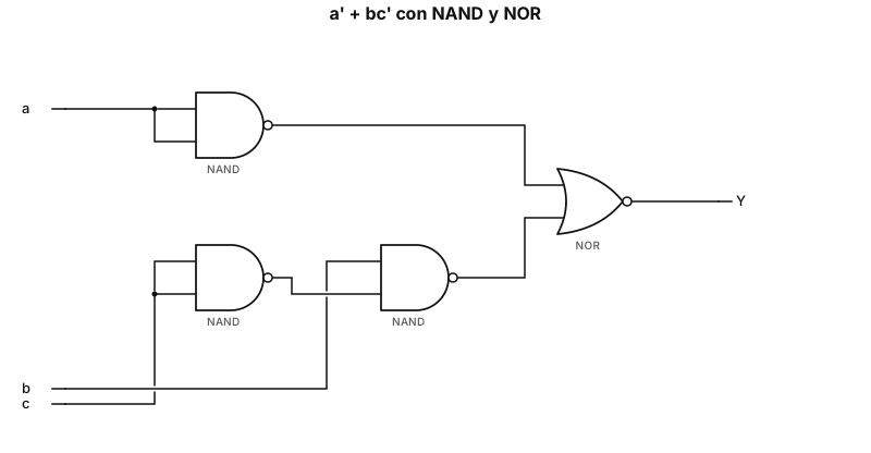
a'+bc' usando compuertas nand y nor
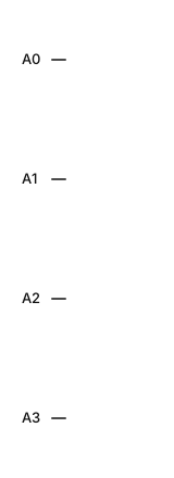
"Generate a logic circuit diagram for a 4-bit Two's Complement generator using a 7483 4-bit binary adder chip. The 4-bit input (A0-A3) goes through 4 NOT gates (inverters) into the A inputs of the 7483 adder. The B inputs (B0-B3) of the 7483 are connected to GND (logic 0). The Carry In (Cin) pin is connected to VCC (logic 1) to add 1. Show outputs S0-S3 and Carry Out (Cout)."
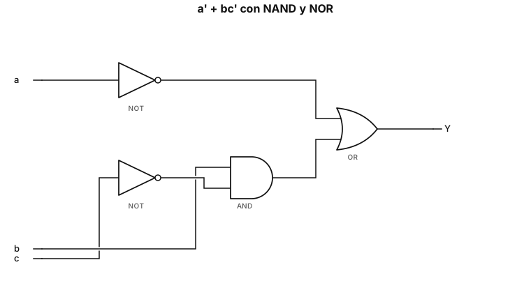
a'+bc' solo con nand y nor
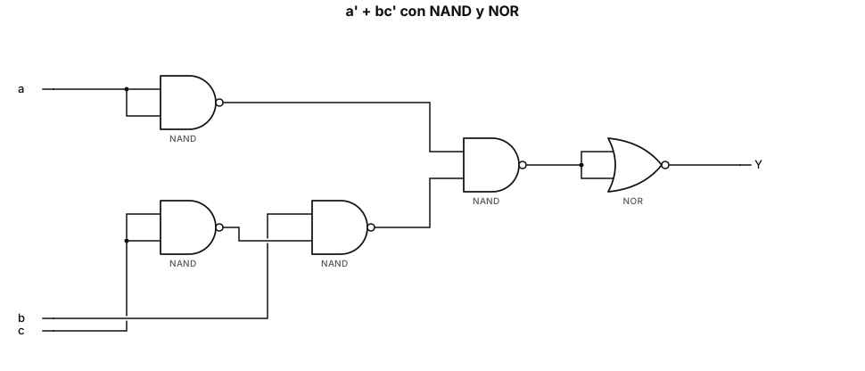
a'+bc' implementado solo con nand y nor
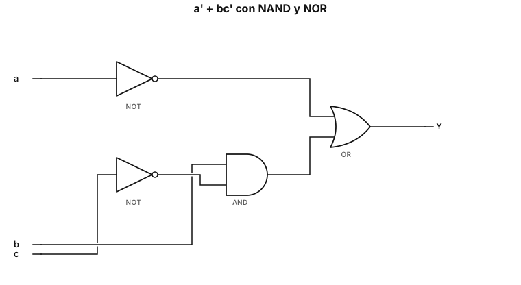
a'+bc' trabaja con nand y nor
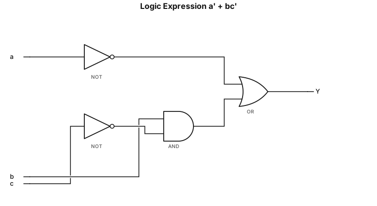
a'+bc'
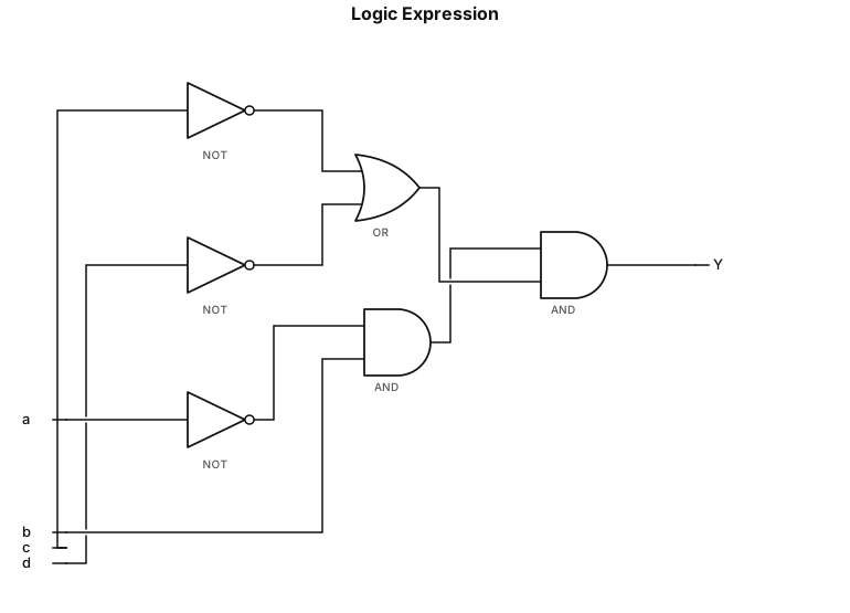
a'b(c'+d')
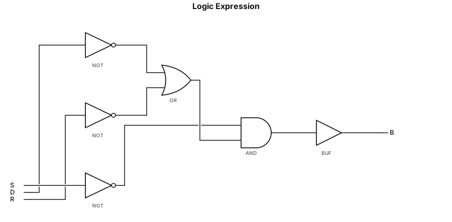
B=V'S(D'+R')
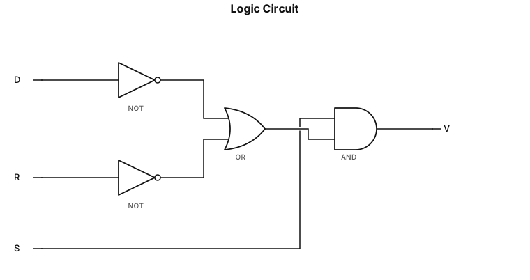
V'S(D'+R')
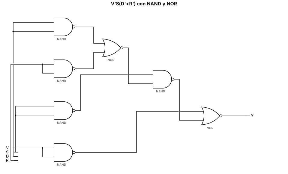
V'S(D'+R') trabajar solo con las compuertas nor y nand
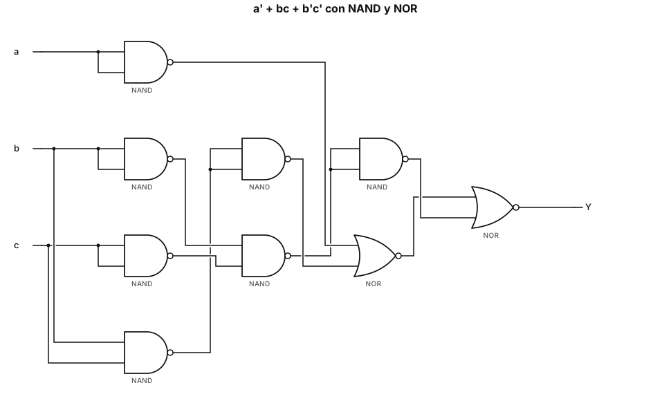
a'+bc+b'c' trabajar solo con las compuertas nor y nand
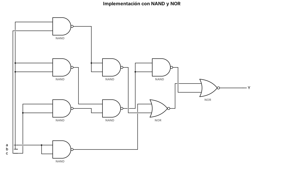
a'+bc+b'c' implementado solo con las compuertas nor y nand

A timing diagram for an I2C read transaction: SCL clock, SDA with START condition, 7-bit address byte, ACK bit, data byte, and STOP condition