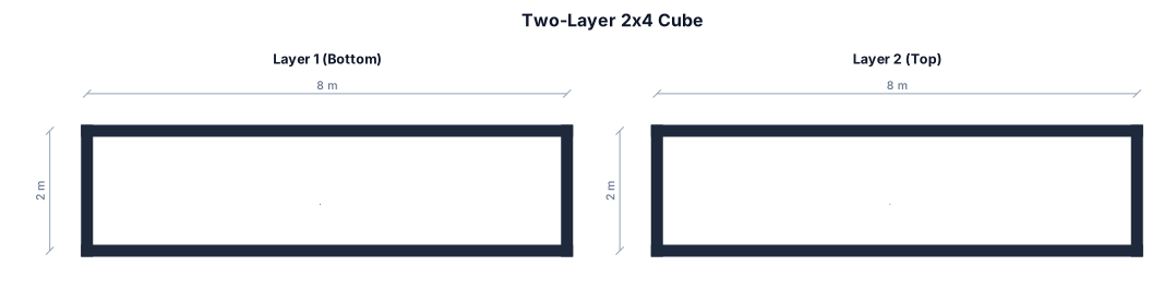
請幫我設計兩層 每層2*4的正方體
NODE ARCHIVE · REAL DIAGRAM BRIEFS
Diagram Examples from Real Visitor Prompts
Browse eligible diagrams shared by FreeDiagram visitors, inspect the exact prompts, and build your own version.
Browse 3310 real creationsCOMMUNITY OUTPUTS · EXACT PROMPTS
All visitor creations
Showing 1897–1920 of 3310. No stock examples or system defaults. Choose a tool, study a real result, then reopen its prompt as your starting point.
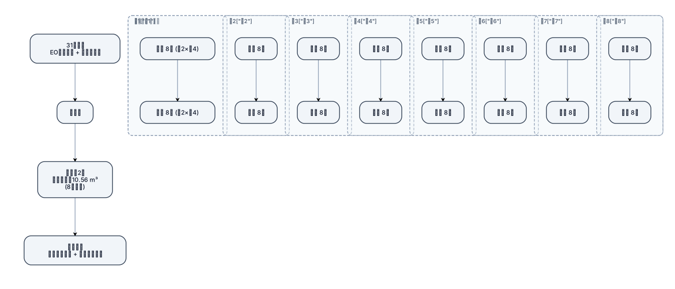
7.4.3.1 共31個點位放置EO指示標籤及生物指示劑,每一層體積為0.66 m3,共8台車,每台車2層產品體積約為10.56m3至少評估,此次執行滲透驗證包含8台車滿載,點位包含四周上下點位及每台車中心點,共計31個點位。 箱體為寬2個*長4個 兩層
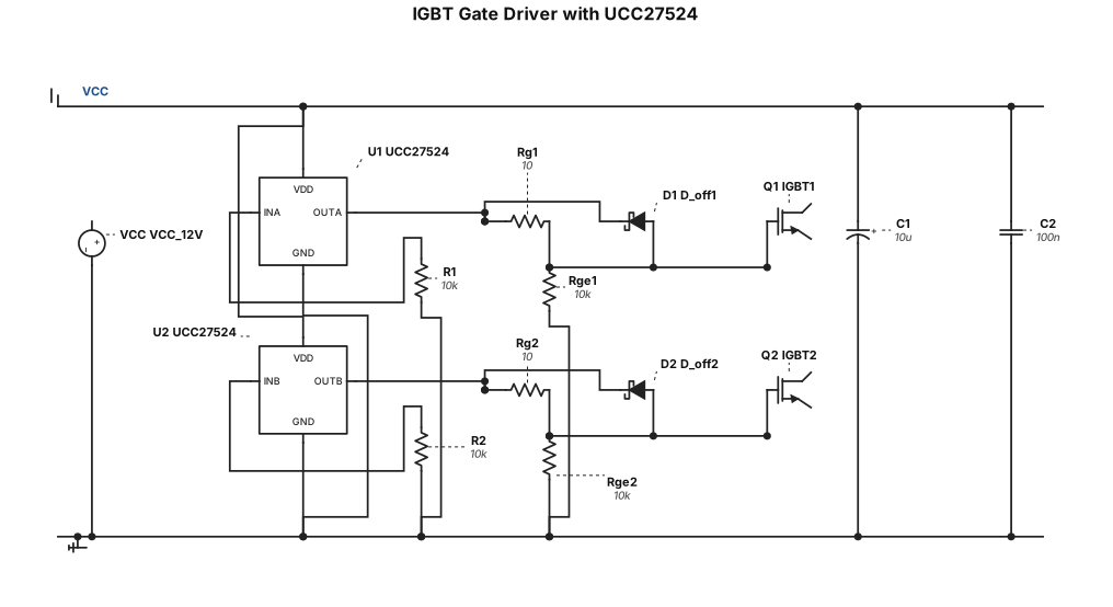
i have to make one circuit using UCC27524 for my IGBT driving applications, suggest circuit
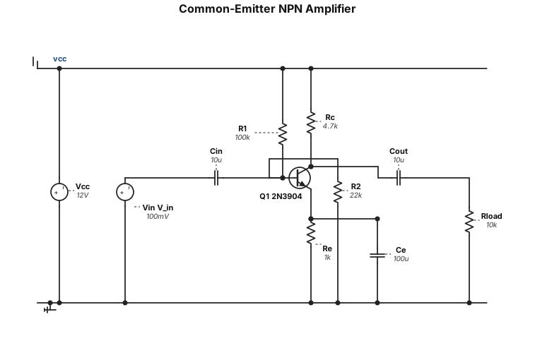
A common-emitter NPN transistor amplifier circuit
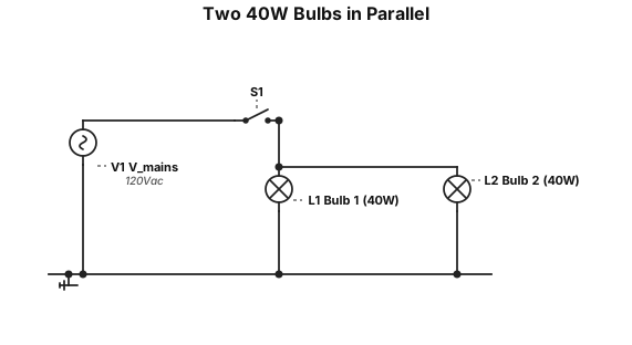
two 40 watt light bulbs connected in parallel in light fixture, powered by 120v of electricity for 150 hours at $0.12 per Kw-hr
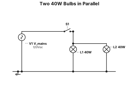
two 40 watt light bulbs connected in parallel in light fixture, powered by 120v of electricity
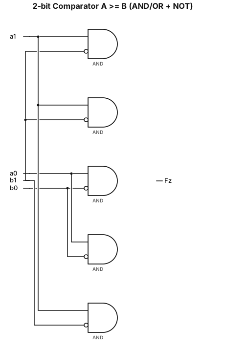
Let A = a1a0 and B = b1b0 be 2-bit unsigned binary numbers. Design a circuit with inputs a1, a0, b1, b0 and output Fz such that: Fz = 1 if and only if A ≥ B. Draw TWO circuit diagrams: (a) Realize the circuit using only AND2 and OR2 gates, with NOT gates allowed for complemented inputs. (b) Realize the circuit using only NAND2 and NOR2 gates. Clearly label every input, intermediate signal, gate, and final output Fz.
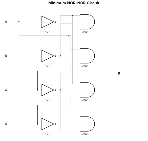
g=A′B′C+AB′C′+A′C′D+AC′D′ draw: Minimum NOR-NOR circuit
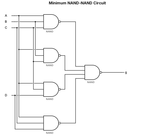
g=A′B′C+AB′C′+A′C′D+AC′D′ draw: Minimum NAND-NAND circuit
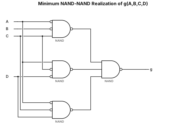
Design the minimum two-level NAND-NAND and NOR-NOR realizations of: g(A,B,C,D) = Σm(2,3,6,8,9,12) Simplify the Boolean function first using a Karnaugh map. Then draw: Minimum NAND-NAND circuit or Problem 3: $$ g(A,B,C,D)=\Sigma m(2,3,6,8,9,12) $$ Minimum SOP equation for NAND-NAND: g= A B C+A B C + A C D+A C D Use only two logic levels and clearly label all complemented inputs, intermediate outputs, and final output g.
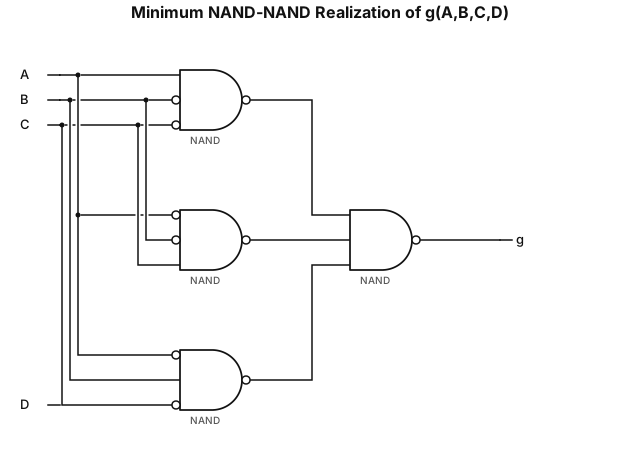
Design the minimum two-level NAND-NAND and NOR-NOR realizations of: g(A,B,C,D) = Σm(2,3,6,8,9,12) Simplify the Boolean function first using a Karnaugh map. Then draw: Minimum NAND-NAND circuit Use only two logic levels and clearly label all complemented inputs, intermediate outputs, and final output g.
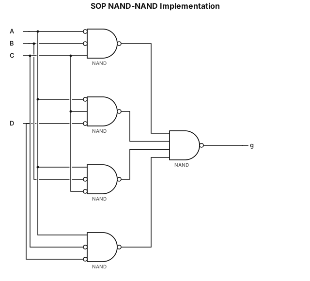
Function: g ( A , B , C , D ) = Σ m ( 2 , 3 , 6 , 8 , 9 , 12 ) g(A,B,C,D)=Σm(2,3,6,8,9,12) Minimum SOP Form (for NAND-NAND): g = A ′ B ′ C + A ′ C D ′ + A B ′ C ′ + A C ′ D ′ g=A ′ B ′ C+A ′ CD ′ +AB ′ C ′ +AC ′ D ′ do not put NOT Gates, simplify wiring
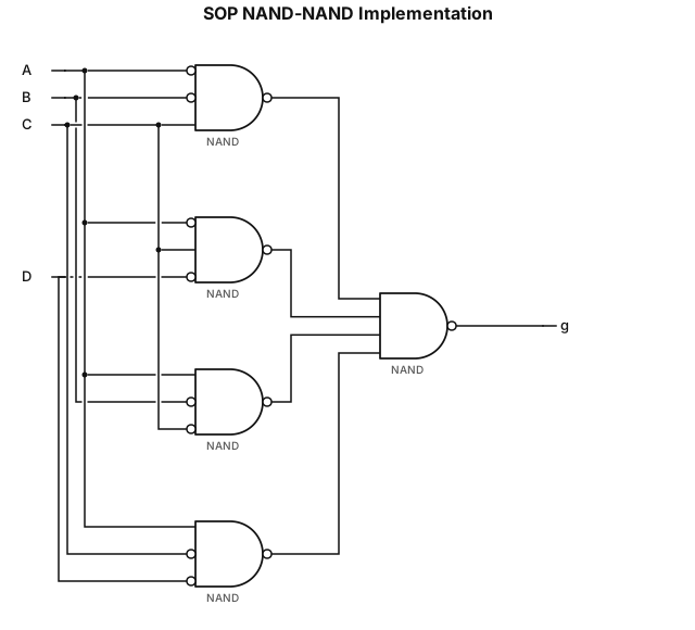
Function: g ( A , B , C , D ) = Σ m ( 2 , 3 , 6 , 8 , 9 , 12 ) g(A,B,C,D)=Σm(2,3,6,8,9,12) Minimum SOP Form (for NAND-NAND): g = A ′ B ′ C + A ′ C D ′ + A B ′ C ′ + A C ′ D ′ g=A ′ B ′ C+A ′ CD ′ +AB ′ C ′ +AC ′ D ′ do not put NOT Gates
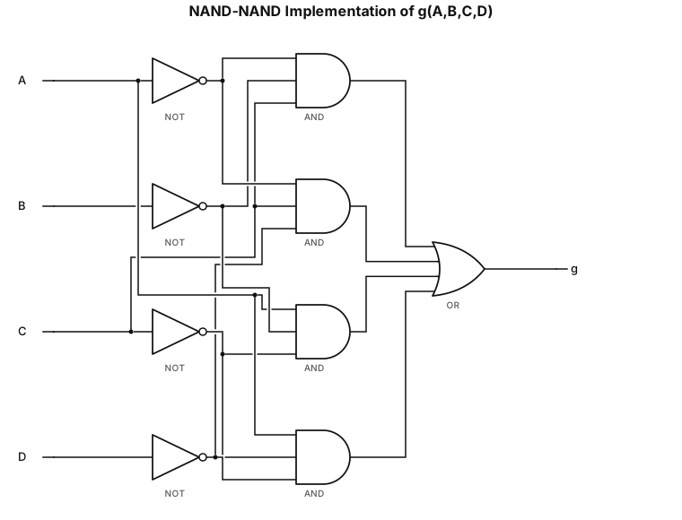
Function: g ( A , B , C , D ) = Σ m ( 2 , 3 , 6 , 8 , 9 , 12 ) g(A,B,C,D)=Σm(2,3,6,8,9,12) Minimum SOP Form (for NAND-NAND): g = A ′ B ′ C + A ′ C D ′ + A B ′ C ′ + A C ′ D ′ g=A ′ B ′ C+A ′ CD ′ +AB ′ C ′ +AC ′ D ′
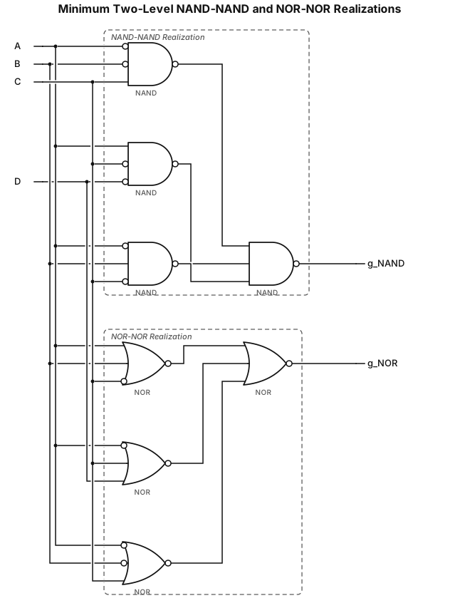
Design the minimum two-level NAND-NAND and NOR-NOR realizations of: g(A,B,C,D) = Σm(2,3,6,8,9,12) Simplify the Boolean function first using a Karnaugh map. Then draw: 1. Minimum NAND-NAND circuit 2. Minimum NOR-NOR circuit Use only two logic levels and clearly label all complemented inputs, intermediate outputs, and final output g.
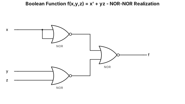
Design the Boolean function f(x,y,z) = x' + yz. Draw TWO circuit diagrams: 1. NOR-NOR realization Use standard logic-gate symbols and clearly label all wires and the final output f.
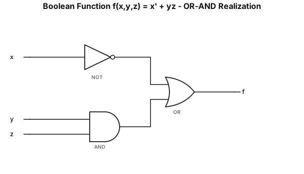
Design the Boolean function f(x,y,z) = x' + yz. Draw TWO circuit diagrams: 1. OR-AND realization Use standard logic-gate symbols and clearly label all wires and the final output f.
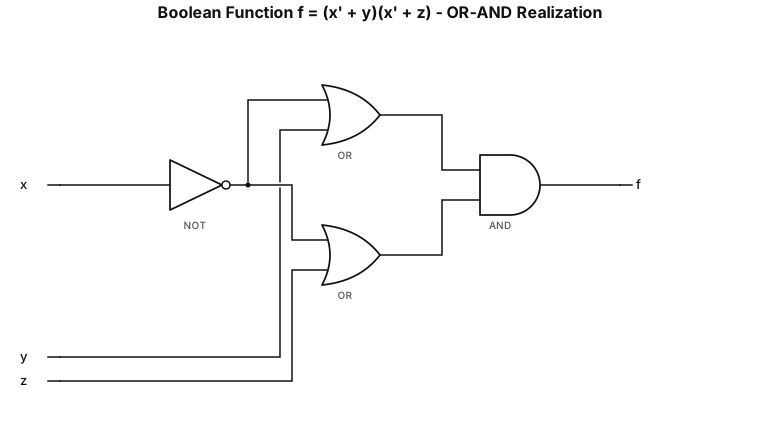
Design the Boolean function f(x,y,z) = x' + yz. First rewrite it as: f = (x' + y)(x' + z) Draw TWO circuit diagrams: 1. OR-AND realization Use standard logic-gate symbols and clearly label all wires and the final output f.
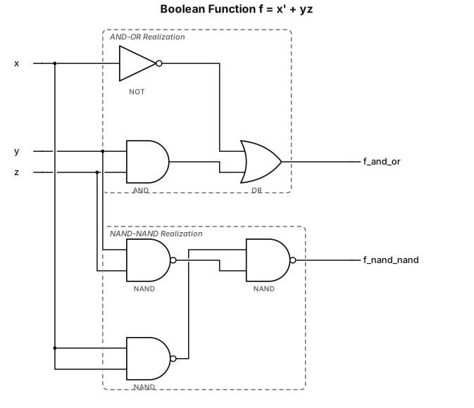
Design the Boolean function f(x,y,z) = x' + yz. Draw TWO circuit diagrams: 1. AND-OR realization 2. NAND-NAND realization Use standard logic-gate symbols, clearly label all inputs, intermediate outputs, and final output f.
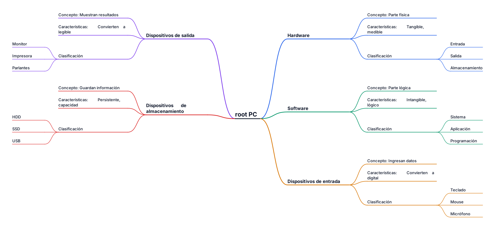
Crea un mapa mental sobre Hardware y Software. La idea central debe ser PC. Incluye Hardware, Software, dispositivos de entrada, salida y almacenamiento. Para cada uno incluye concepto, características y clasificación. Usa pocas palabras, colores diferentes por rama y un diseño apropiado para una tarea universitaria.
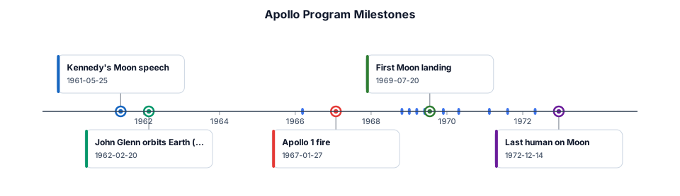
A timeline of the Apollo program's major milestones from 1961 to 1972, including key missions and the first moon landing

Create a simple oil and gas condensate transfer P&ID for an educational demo. Title: CONDENSATE TRANSFER - DEMO ONLY. Left to right: storage tank TK-101, manual isolation valve HV-101, centrifugal pump P-101, check valve NRV-101, flow transmitter FT-101, control valve FCV-101, and receiving tank TK-102. Connect the equipment with solid process piping and flow arrows. Show a dashed electrical signal from FT-101 to flow indicating controller FIC-101 and then to FCV-101. Keep the layout clean, readable and compact with equipment and instrument tags. Add note: CONCEPT ONLY - NOT FOR CONSTRUCTION. Do not invent pressure ratings, dimensions, or engineering calculations.
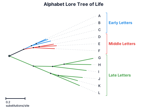
Alphabet lore tree of life
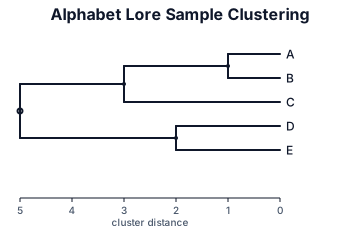
Alphabet lore sample clustering