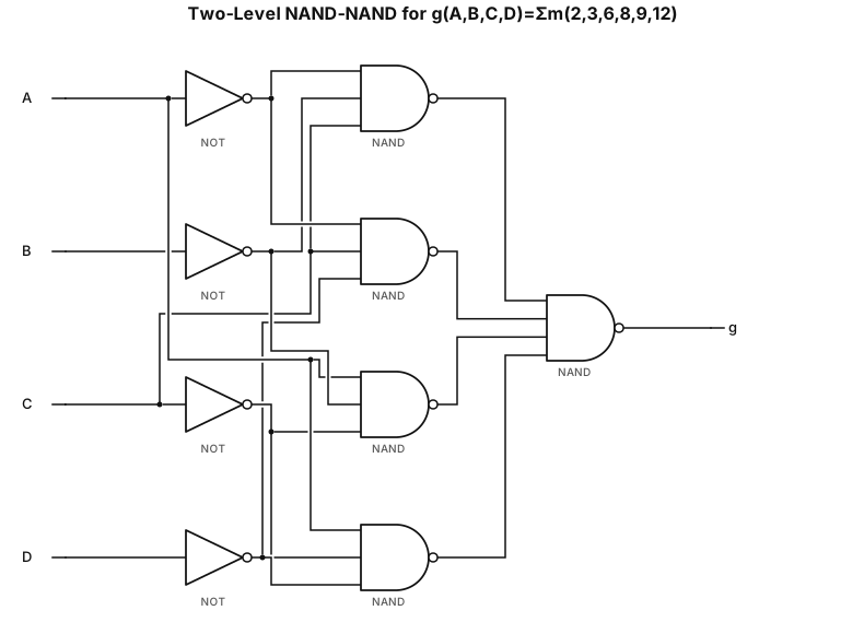
Draw a standard two-level NAND-NAND circuit for g(A,B,C,D)=Σm(2,3,6,8,9,12). First use four separate NOT gates to create A’, B’, C’, and D’. Then use exactly four 3-input NAND gates: NAND1 inputs A’, B’, C; NAND2 inputs A’, C, D’; NAND3 inputs A, B’, C’; NAND4 inputs A, C’, D’. Connect the outputs of these four NAND gates to one final 4-input NAND gate producing g. Do NOT use input bubbles. Use explicit NOT gate symbols for all complemented variables. Label every signal clearly and clean up the crossing wires
NODE ARCHIVE · REAL DIAGRAM BRIEFS
Diagram Examples from Real Visitor Prompts
Browse eligible diagrams shared by FreeDiagram visitors, inspect the exact prompts, and build your own version.
Browse 3310 real creationsCOMMUNITY OUTPUTS · EXACT PROMPTS
All visitor creations
Showing 1921–1944 of 3310. No stock examples or system defaults. Choose a tool, study a real result, then reopen its prompt as your starting point.
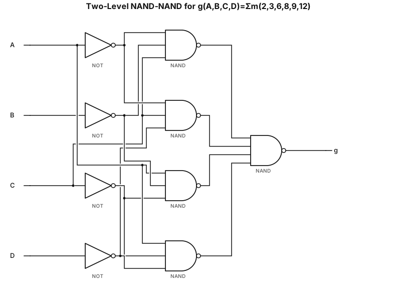
Draw a standard two-level NAND-NAND circuit for g(A,B,C,D)=Σm(2,3,6,8,9,12). First use four separate NOT gates to create A’, B’, C’, and D’. Then use exactly four 3-input NAND gates: NAND1 inputs A’, B’, C; NAND2 inputs A’, C, D’; NAND3 inputs A, B’, C’; NAND4 inputs A, C’, D’. Connect the outputs of these four NAND gates to one final 4-input NAND gate producing g. Do NOT use input bubbles. Use explicit NOT gate symbols for all complemented variables. Label every signal clearly.
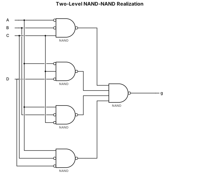
Draw a minimum two-level NAND-NAND realization for g(A,B,C,D)=\Sigma m(2,3,6,8,9,12). Use the SOP expression g=A'B'C+A'CD'+AB'C'+AC'D'. Draw exactly four first-level NAND gates, one for each product term, followed by one final NAND gate. Clearly label A, B, C, D and all complemented inputs.
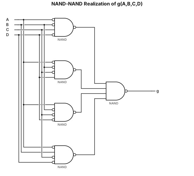
3. Design minimum two-level NAND-NAND and NOR-NOR realizations of the function g(A, B, C, D) = ∑m(2,3,6,8,9,12)
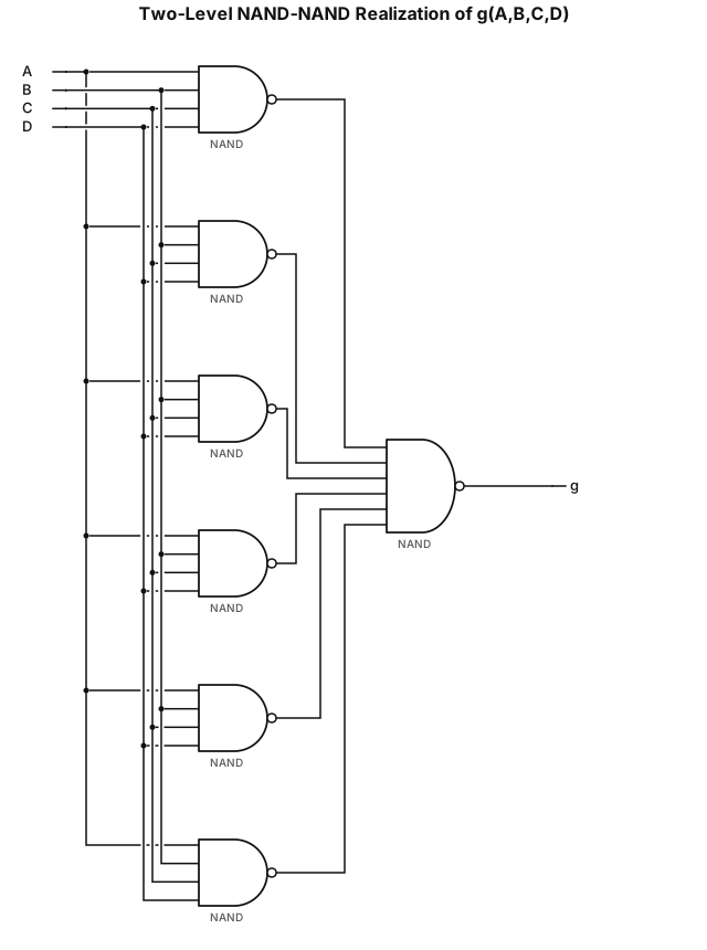
Design minimum two-level NAND-NAND realizations of the function g(A, B, C, D) = ∑m(2,3,6,8,9,12)
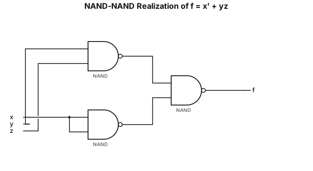
NAND-NAND realizations of f=x’+yz
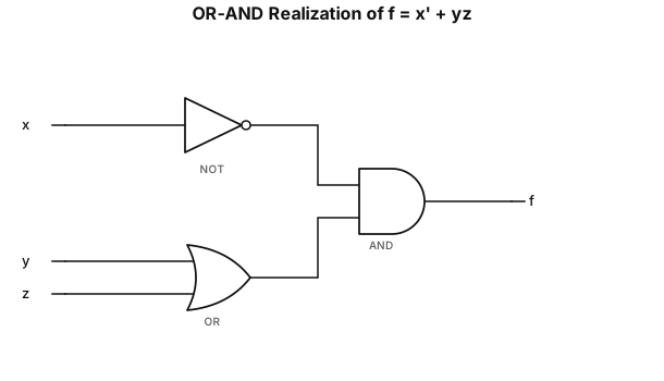
OR-AND realizations of f=x’+yz
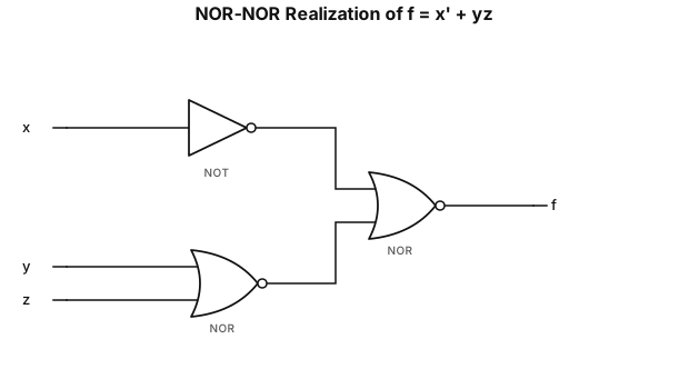
NOR-NOR realizations of f=x’+yz
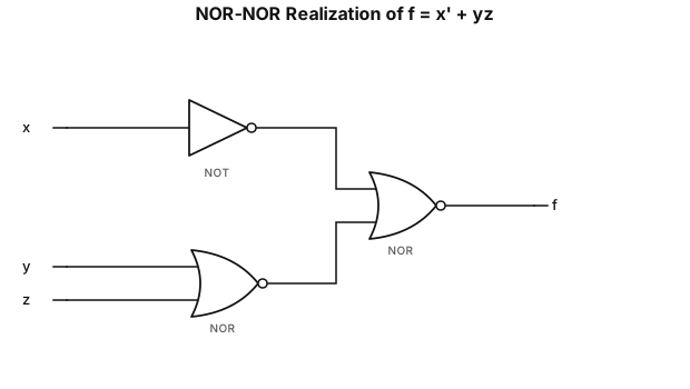
Draw NOR-NOR realizations of f=xbar+yz
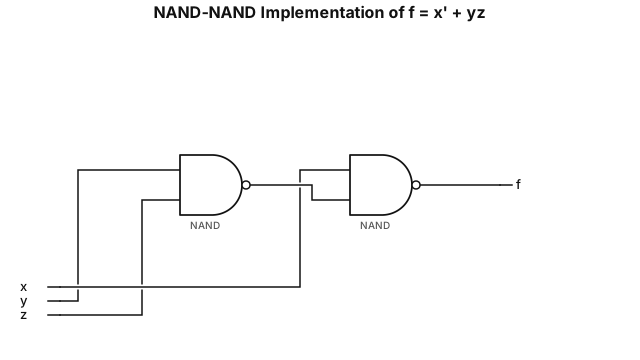
NAND-NAND of f=xbar+yz
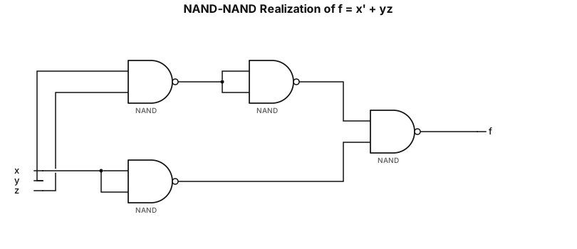
NAND-NAND realizations of the logic function f(x, y, z) = xbar+ yz. Draw the circuit diagrams.
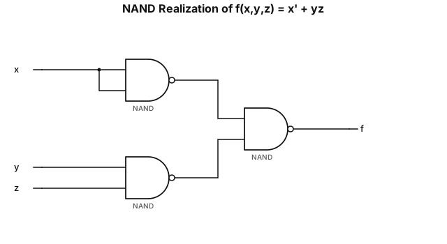
NAND nandrealizations of the logic function f(x, y, z) = xbar+ yz. Draw the circuit diagrams.
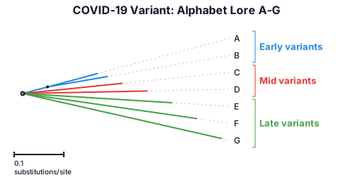
COVID-19 variant: alphabet lore A-G
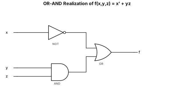
OR-AND realizations of the logic function f(x, y, z) = xbar+ yz. Draw the circuit diagrams.
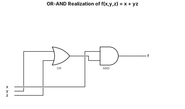
OR-AND realizations of the logic function f(x, y, z) = x + yz. Draw the circuit diagrams.
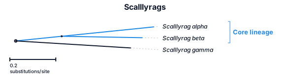
Scalllyrags
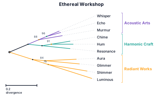
Ethereal workshop
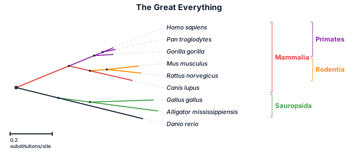
A phylogenetic tree of the great everything
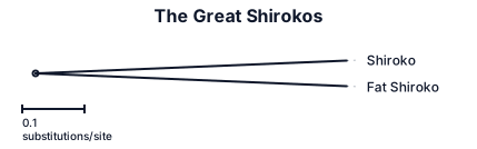
A phylogenetic tree of the great shirokos: shiroko‚ fat shiroko
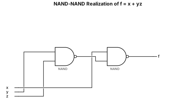
NAND-NAND realizations of the logic function f(x, y, z) = x + yz. Draw the circuit diagrams.
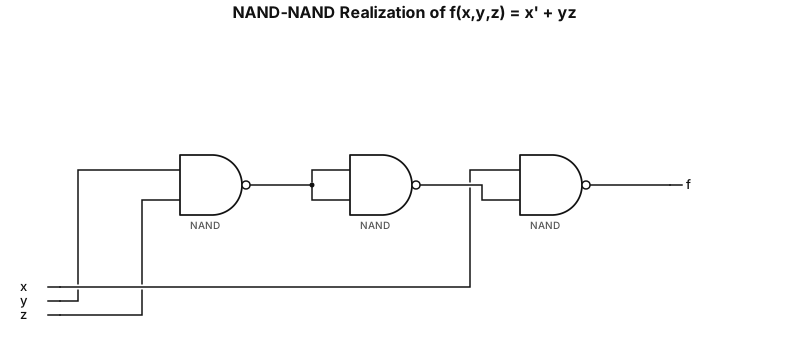
Design NAND-NAND realizations of the logic function f(x, y, z) = xbar+ yz. Draw the circuit diagrams. Make it clear please
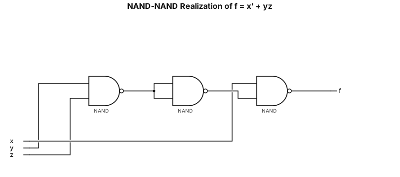
Design NAND-NAND realizations of the logic function f(x, y, z) = xbar+ yz. Draw the circuit diagrams.
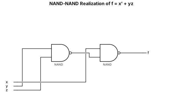
Design NAND-NAND realizations of the logic function f(x, y, z) = xbar + yz. Draw the circuit diagrams.
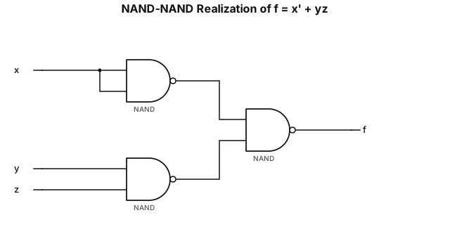
Design NAND- NAND realizations of the logic function f(x, y, z) = xbar + yz. Draw the circuit diagrams.